Data cache method used in NAND FLASH

A data cache and cache technology, applied in electrical digital data processing, memory systems, instruments, etc., can solve problems such as inability to effectively improve the write performance of SSD systems, reduce cache hit rates, and increase garbage collection costs, and achieve the speed of random access. Fast, effective cache data management, excellent replacement effect

Active Publication Date: 2016-09-07
BEIJING MXTRONICS CORP +1
View PDF4 Cites 23 Cited by
  • Summary
  • Abstract
  • Description
  • Claims
  • Application Information

AI Technical Summary

Problems solved by technology

However, these methods still have the problem of write penalty and write amplification. Sectors or pages are used as the internal read and write granularity of SSD. The page filling process increases the cache management mapping table space consumption, reduces the cache hit rate, and also increases garbage. The cost of recovery can not effectively improve the write performance of SSD system

Method used


Image

  • Data cache method used in NAND FLASH
  • Data cache method used in NAND FLASH
  • Data cache method used in NAND FLASH

Examples


Embodiment Construction

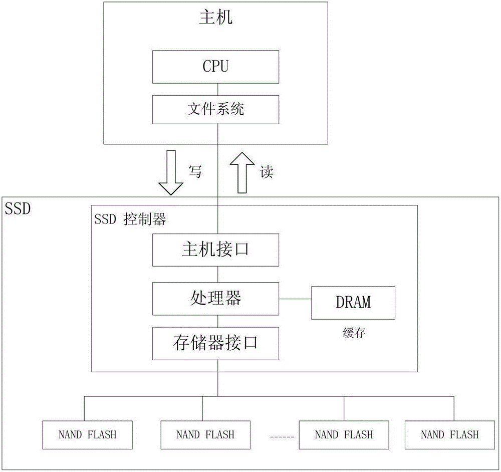
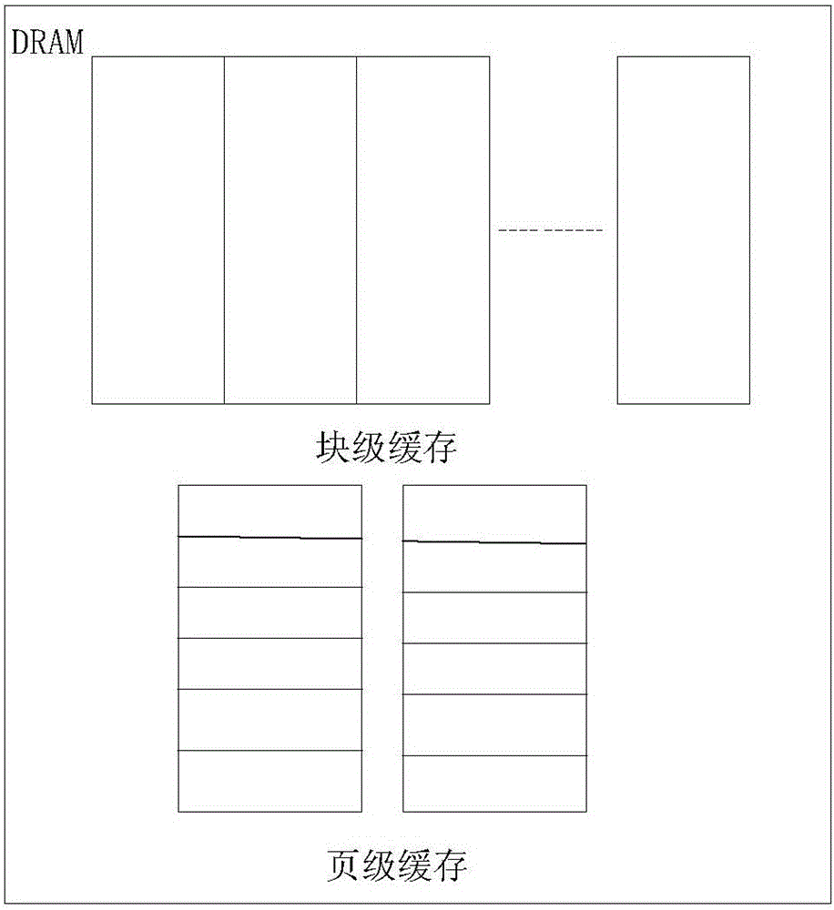
[0038] The present invention is aimed at the deficiencies in the prior art, proposes a kind of data cache method for NAND FLASH, the method of the present invention is applicable to the data reading and writing of SSD, such as figure 1 Shown is a system structure diagram of the method of the present invention, the host controls the SSD to perform data read and write operations, the host includes a CPU and a file system, the SSD includes an SSD controller, and a NAND FLASH chip, and the host interface in the SSD controller is responsible for communicating with the host. The storage interface is responsible for communicating with FLASH, the processor is responsible for timing control and space control, and the DRAM data buffer is responsible for caching read and write data. When the host side reads and writes data to the SSD, the smallest unit of data is a sector. Each page in the SSD is composed of sectors, and each block is composed of multiple pages. For example, the size of a...


PUM


Abstract

The invention provides a data cache method used in NAND FLASH. The method comprises following steps: first, a cache region cache is divided into a block-level cache and a page-level cache; then, when read-and write is performed on data, if current data exists in the block-level cache or the page-level cache, then data read-and write is directly completed; if current data does not exist in the block-level cache or the page-level cache, then data is read from the FLASH or free space in the data cache region is distributed to the current data and data is written in the FLASH; if there is no free space, a substitution block is determined through a substitution algorithm and data in the substitution block is written in the FLASH; finally, the substitution block is released, new data is written in, and then data cache is completed. By means of the combination of block cache and page cache, the cache hit ratio of random read-and-write access is increased; a efficient substitution algorithm is provided; the size of cache mapping table is reduced and space utilization rate of the cache region is increased; the method has good use value.

Description

technical field [0001] The invention relates to a FLASH storage technology, in particular to a data cache method for NAND FLASH. Background technique [0002] At present, relatively mainstream SSDs are all based on NAND FLASH media. SSDs include main control, flash memory, cache, and firmware. Due to the structural characteristics of NAND FLASH, the basic unit of erasing operation is block, while the basic unit of reading and writing is page, and the smallest unit of reading and writing data from host to SSD is sector. Therefore, FLASH needs to erase the block before writing data, and copy other valid data to the free block before erasing, and then write other valid data and rewritten data into the block after the erase is completed. [0003] In the traditional read and write technology, the host generally uses the following method to write data to the SSD: the host first writes the data into the cache through the storage array, and then writes the data to the SSD after the...

Claims


Application Information

Patent Timeline
Patent Type & Authority Applications(China)
IPC IPC(8): G06F12/0897
CPCG06F12/0897
Inventor 赵微张志永宗宇
Owner BEIJING MXTRONICS CORP
Why Eureka
Try Eureka