Liquid crystal display panel

A liquid crystal display panel and display area technology, applied in static indicators, nonlinear optics, instruments, etc., can solve the problems of electrostatic discharge damage, light leakage of display panels, etc., to reduce electrostatic discharge damage, avoid electrostatic discharge damage, The effect of reducing inconsistencies

Active Publication Date: 2009-09-23
AU OPTRONICS CORP
View PDF7 Cites 0 Cited by
  • Summary
  • Abstract
  • Description
  • Claims
  • Application Information

AI Technical Summary

Problems solved by technology

[0009] The object of the present invention is to provide a liquid crystal display panel, which forms a light-shielding pattern across the scanning wiring and data wiring at the edge of the panel, so as to solve the situation that light leakage is prone to occur at the edge of the display panel, and can avoid Situations where ESD damage may result from the use of multiple floating metals in the prior art

Method used


Image

  • Liquid crystal display panel
  • Liquid crystal display panel
  • Liquid crystal display panel

Examples


Embodiment Construction

[0056] In order to make the above and other objects, features and advantages of the present invention more comprehensible, preferred embodiments are described below in detail with accompanying drawings.

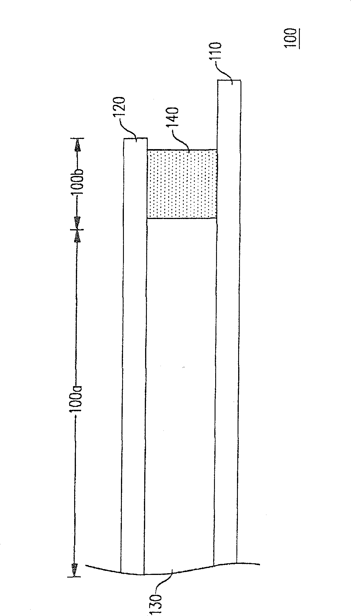
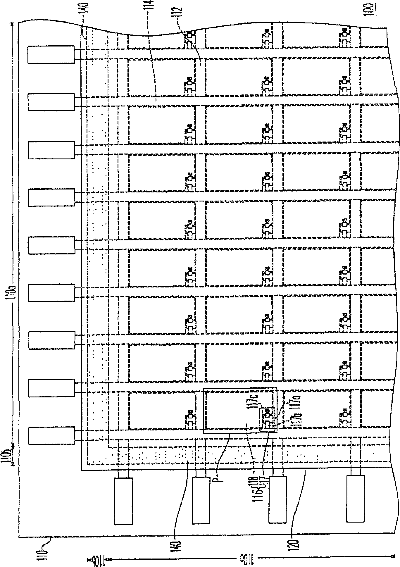
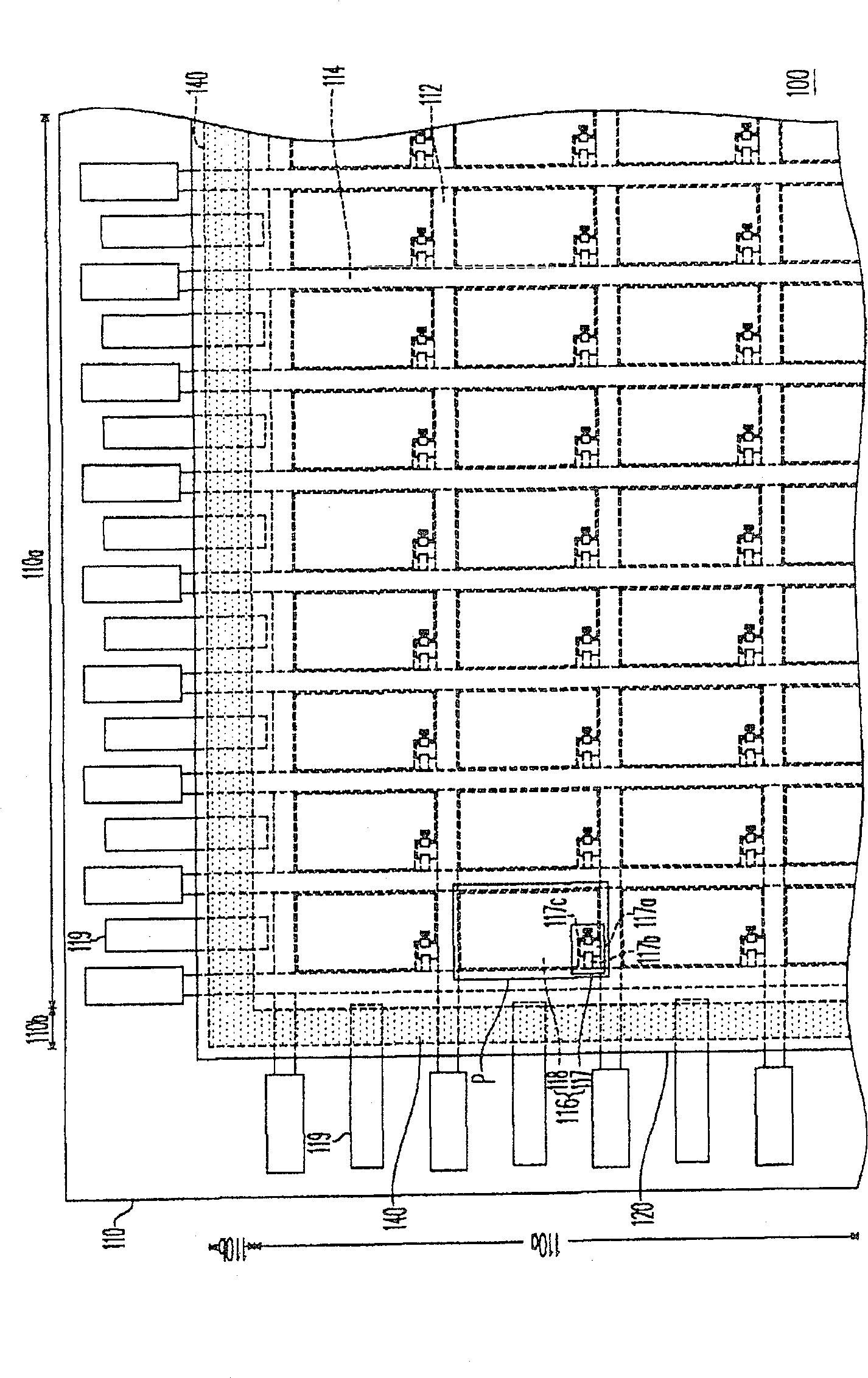
[0057] Figure 3A is a schematic top view of a liquid crystal display panel according to the first embodiment of the present invention; Figure 3B for along Figure 3A The cross-sectional schematic diagram of the thin film transistor array substrate and the sealant part drawn by the I-I' section line; Figure 3C for along Figure 3A The cross-sectional schematic diagram of the thin film transistor array substrate and the frame glue part drawn by the II-II' section line. First, please refer to Figure 3A The liquid crystal display panel 200 is mainly composed of a thin film transistor array substrate 210 , a color filter substrate 220 , a frame glue 230 and a liquid crystal layer (not shown). The color filter substrate 220 is disposed above the TFT array substrate 210 . ...


PUM


Abstract

The invention provides a liquid crystal display panel, which mainly includes a thin film transistor array substrate, a color filter substrate, a frame glue and a liquid crystal layer. Among them, the thin film transistor array substrate includes a substrate, multiple pixel structures, multiple scanning lines, multiple data lines and a light-shielding pattern. The scanning lines and data lines are arranged on the substrate to control the operation of the pixel structure. The light-shielding pattern is arranged on the edge of the panel, straddles the scanning wiring and the data wiring, and is electrically insulated from the scanning wiring and the data wiring. The sealant is arranged between the thin film transistor array substrate and the color filter substrate, and corresponds to the light-shielding pattern. The liquid crystal layer is arranged between the color filter substrate, the thin film transistor array substrate and the frame glue.

Description

technical field [0001] The present invention relates to a liquid crystal display panel, and in particular to a liquid crystal display panel (LIQUID CRYSTALDISPLAY PANEL) with a light-shielding pattern on the edge. Background technique [0002] The rapid progress of the multimedia society is mostly due to the rapid progress of semiconductor components and display devices. As far as display panels are concerned, thin film transistor liquid crystal display panels (Thin Film Transistor Liquid Crystal Display, TFT LCD) with superior characteristics such as high image quality, good space utilization efficiency, low power consumption, and no radiation have gradually become the mainstream of the market. [0003] Generally speaking, a thin film transistor liquid crystal display panel is composed of a thin film transistor array substrate, a color filter substrate, and a liquid crystal layer sandwiched between the two substrates. The surface of the thin film transistor array substrate...

Claims


Application Information

Patent Timeline
Patent Type & Authority Patents(China)
IPC IPC(8): G02F1/1362G02F1/1335G02F1/133
Inventor 李豪捷施明宏
Owner AU OPTRONICS CORP
Why Eureka
Try Eureka