
Configurable logic component without a local configuration memory and with a parallel configuration bus

A technology for configuring logic and memory, applied in the direction of logic circuits using specific components, logic circuits using basic logic circuit components, logic circuits, etc.

Inactive Publication Date: 2009-10-28
INFINEON TECH AG
View PDF4 Cites 0 Cited by
  • Summary
  • Abstract
  • Description
  • Claims
  • Application Information

AI Technical Summary

Problems solved by technology

An important and very expensive disadvantage of this solution, however, is the need to combine two different semiconductor technologies on one chip and allow one to optimize the EEPROM cells and configurable The semiconductor technology of the unit is available in both

Method used


Image

  • Configurable logic component without a local configuration memory and with a parallel configuration bus
  • Configurable logic component without a local configuration memory and with a parallel configuration bus
  • Configurable logic component without a local configuration memory and with a parallel configuration bus

Examples


Embodiment Construction

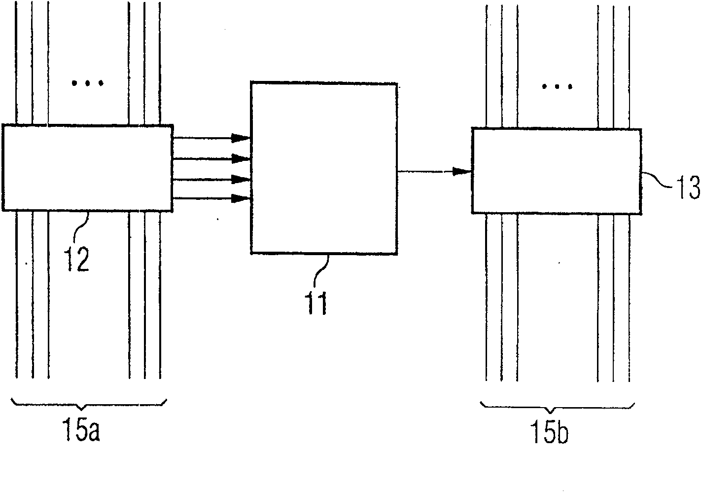
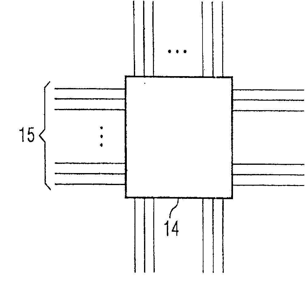
[0059] Generally speaking, there are four types of cells generated in a logic device, for example, a programmable logic device or a field programmable gate array (FPGA), in Figure 1A and Figure 1B depicted in . The configurable logic unit 11 is used for signal processing in this bit stage. The configurable tap unit 12 switches on as many signals as the configurable logic unit 11 has inputs from a data bus 15a. The configurable supply unit 13 supplies the output of the configurable logic unit 11 to a further data bus 15b. The configurable association unit 14 is a matrix for the selectivity and bidirectional switching of signal paths (wires) in a connection network of logic components 30 .

[0060] A typical implementation of the configurable logic unit 11 uses look-up tables (lut). In the following, a look-up table (lut4) with four input signals and one output signal is assumed as an example. The table requires 16 configuration signals for unrestricted setting capabilitie...


PUM


Abstract

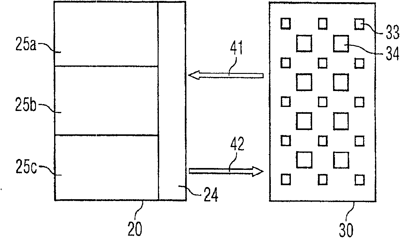
The invention relates to a configurable logic module without local configuration memory but with parallel configuration bus. A configurable logic component (30) that does not contain a configuration memory. The configuration of the configurable logic component is defined by the applied voltage. The configuration voltage is preferably generated in an external configuration memory (2). In a preferred embodiment, a memory chip (20) (for example, Electrically Erasable Programmable Read-Only Memory (EEPROM)) is mounted face-to-face with the logic components of the present invention without a configuration memory (30) . An intermediate structured solder layer (40) enables multiple electrical connections.

Description

technical field [0001] The invention relates to simplified devices and methods for rapidly reprogramming a programmable logic device (PLD) according to the separate claim. Background technique [0002] Programmable Logic Devices (PLD, Programmable Logic Devices) are generic constructions that often have a very regular structure for logic operations. They include a plurality of switches, which can switch a plurality of signal paths. Therefore, they only receive their specific functions via configuration. A programmable logic device (PLD) ( Figure 1A and 1B ) essentially consists of a configurable logic unit, and a configurable connection network that allows the logic unit to be logically connected as required. The configuration of the programmable logic device (PLD) is here related to the possibility of complex configurations of both the logic cell and the connection network, either at the bit level or at a somewhat complex cell level. The more commonly used approach on ...

Claims


Application Information

Patent Timeline
Patent Type & Authority Patents(China)
IPC IPC(8): G06F17/50H03K19/177H03K19/173
CPCH03K19/17748H03K19/1731H03K19/17796H03K19/17704H03K19/1776
Inventor M·舍普勒W·格鲁伯
Owner INFINEON TECH AG
Learn More