Semiconductor chip comb sliver repairing method and device

A semiconductor and sliver technology, which is applied in the field of semiconductor chip sliver repair and device, can solve the problems of sliver processing that does not meet the requirements, cannot meet the production capacity, and is prone to operating errors, etc., so as to improve the repair efficiency and achieve small and compact dimensions. , good matching effect

Active Publication Date: 2009-11-04
ZHUZHOU CRRC TIMES SEMICON CO LTD
View PDF5 Cites 0 Cited by
  • Summary
  • Abstract
  • Description
  • Claims
  • Application Information

AI Technical Summary

Problems solved by technology

However, due to various factors in the processing, it is inevitable that some sliver processing does not meet the requirements in the processing. Since the value of these semiconductor chips is very expensive, in order to prevent this part of the semiconductor chip from being discarded, it is necessary to process the sliver. Further repairs to remove unqualified slivers and restore semiconductor chips to qualified requirements
At present, unqualified slivers in devices such as GCT / GTO are removed under a microscopic operating table and manually with a scalpel. The main disadvantage of this repair method is that it is difficult to operate and prone to operational errors, especially With the continuous expansion of the amount of semiconductor chip processing, this manual repair method can no longer meet the requirements of production capacity, so it needs to be improved
No relevant patent literature reports have been found through domestic patent searches

Method used


Image

  • Semiconductor chip comb sliver repairing method and device
  • Semiconductor chip comb sliver repairing method and device
  • Semiconductor chip comb sliver repairing method and device

Examples


Embodiment Construction

[0014] The present invention will be further described below in conjunction with the accompanying drawings and embodiments.

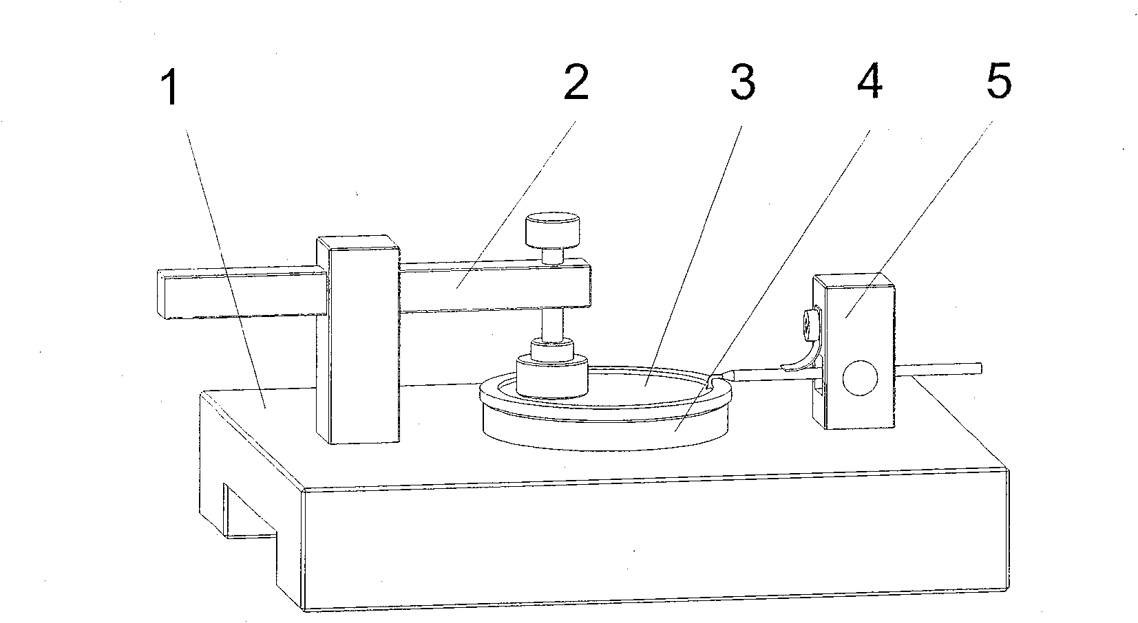
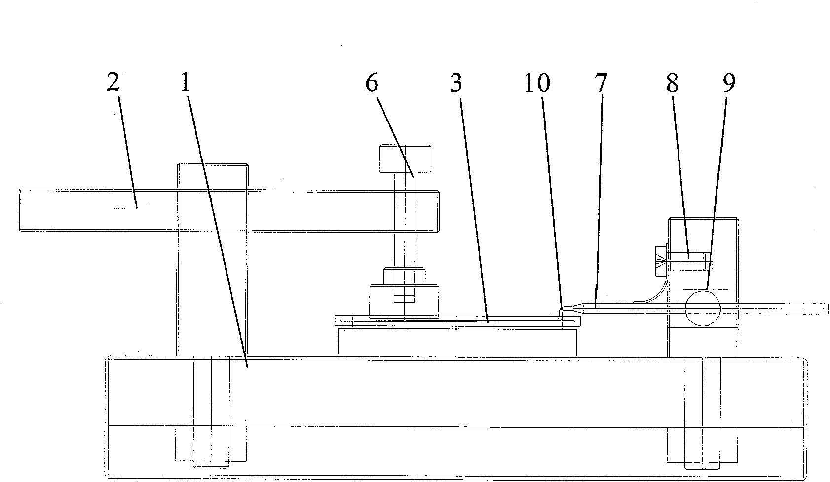
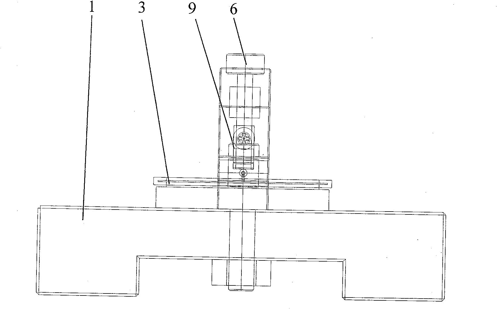
[0015] pass figure 1 It can be seen that the present invention is a chip sliver repair device for semiconductor devices. The repair device uses a sliver repair mechanism simulating a manual repair method to repair problematic sliver. The simulated manual repair method uses a set of sliver repair mechanism arranged on a microscopic workbench to simulate the manual repair method to repair the sliver. The specific repair method can be that a positioning device fixes the semiconductor device chip, and then completes the repair of the chip sliver by a set of picking and combing mechanism simulating manual repair of the chip sliver. Wherein, the combing mechanism for simulating the manual repair of the chip comb is to adjust the knife edge of the repairing comb to the root of the comb to be combed and to align with the length direction of the comb through a ...


PUM


Abstract

The semiconductor chip sliver repair method and device repair the problematic sliver through a set of sliver repair mechanism simulating the manual repair method. The simulated manual repair method is to fix the semiconductor device chip on the microscopic workbench through a set of positioning devices, and then complete the repair of the chip sliver by a set of picking and combing mechanism that simulates manual repairing of the chip sliver. Wherein, the combing mechanism for simulating manual chip repairing is to adjust the knife edge of the repairing sliver to the root of the sliver to be slivered and to align with the length direction of the sliver through a micro-motion positioning mechanism, so as to prepare for slitting ; Then the bolt guide mechanism installed together with the cutter makes the knife edge produce the required linear motion to complete the action of removing the sliver. The sliver repair mechanism is composed of a chip positioning seat, a cutter, a micro-motion positioning mechanism and a fastening guide mechanism, and the whole structure is placed in the "microscopic workbench".

Description

technical field [0001] The invention relates to a semiconductor device processing method and device, in particular to a semiconductor device chip comb repair method and repair device. The technology of the invention is mainly used for high-power semiconductor thyristors with combs on the chip, and can also be used for repairing the combs of other semiconductor elements. Background technique [0002] There are combs on the surface of the chips of many semiconductor devices (such as GCT, GTO, etc.). These combs are important structures that constitute semiconductor devices. It is an important indicator of the normal operation of the product, so the processing requirements for the semiconductor chip sliver are very strict in the processing technology. However, due to various factors in the processing, it is inevitable that some sliver processing does not meet the requirements in the processing. Since the value of these semiconductor chips is very expensive, in order to prevent...

Claims


Application Information

Patent Timeline
Patent Type & Authority Patents(China)
IPC IPC(8): H01L21/02
Inventor 张明李继鲁蒋谊陈芳林
Owner ZHUZHOU CRRC TIMES SEMICON CO LTD
Why Eureka
Try Eureka