Scan driver for selectively performing progressive scanning and interlaced scanning and display using the same
A scanning driver, progressive scanning technology, applied in the field of scanning drivers, can solve the problem that FDP does not include progressive scanning and interlaced scanning scanning drivers, etc.
- Summary
- Abstract
- Description
- Claims
- Application Information
AI Technical Summary
Problems solved by technology
Method used
Image
Examples
Embodiment 2
[0083] Figure 5A is a block diagram of an organic electroluminescent (EL) display including a scan driver according to another exemplary embodiment of the present invention, and Figure 5B yes Figure 5A The circuit diagram of the pixel driving circuit of the organic EL display shown.
[0084] refer to Figure 5A , the organic EL display includes a scan driver 301 , a data driver 303 , and a pixel array 305 .
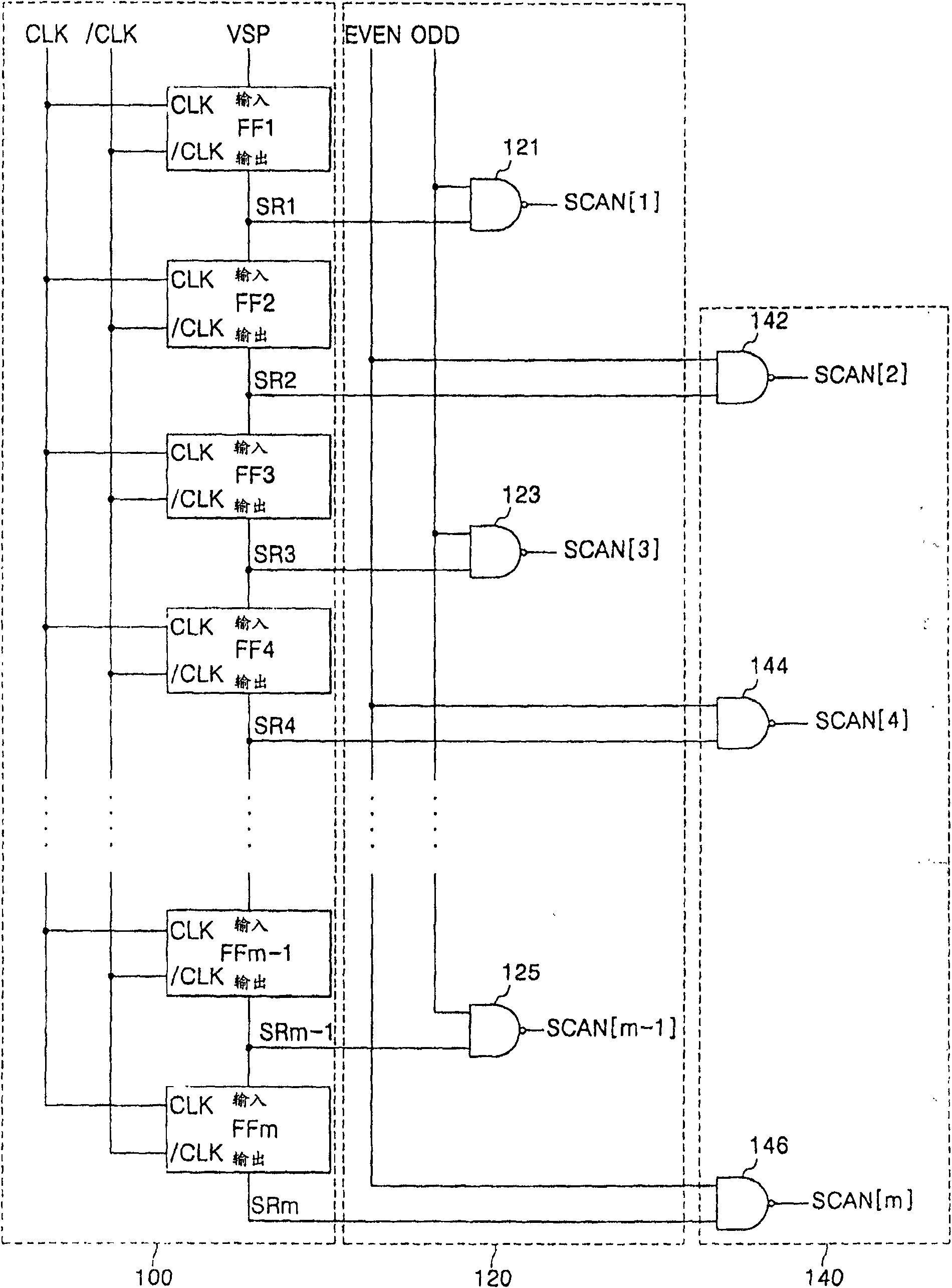
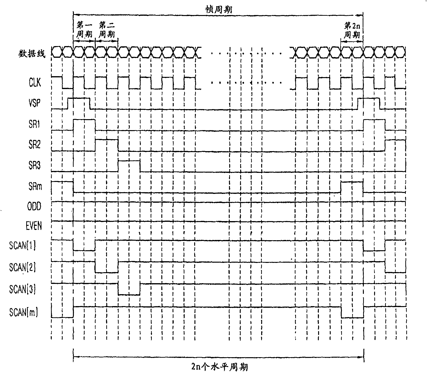
[0085] The scan driver 301 selectively executes figure 1 Progressive scan and interlaced scan are shown. The scan driver 301 also applies scan signals via m scan lines, and applies emission control signals via m emission control lines.
[0086] The data driver 303 applies data to the lines of the pixel array 305 selected by the emission control signal and the scan signal. The applied data can be voltage or current. When the applied data is a voltage, the organic EL display may be a voltage writing type, and when the applied data is a current, the organic EL disp...
Embodiment 3
[0122] Figure 7 is a circuit diagram of a scan driver according to another exemplary embodiment of the present invention.
[0123] refer to Figure 7 , the scan driver includes a shift register 400 , a mode selection unit 420 , an odd line selection unit 440 , and an even line selection unit 460 .
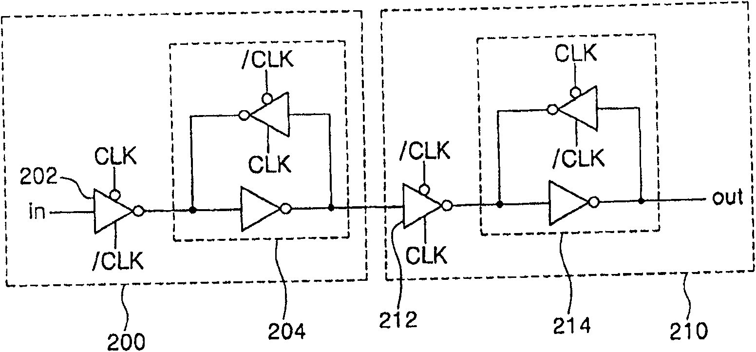
[0124] The shift register 400 includes a plurality of flip-flops, and there are more flip-flops than scan lines of the panel. Thus, when the panel includes m scan lines, the shift register 400 includes at least m+1 flip-flops. At least one of the clock signal CLK and the inverted clock signal / CLK is input to each flip-flop.
[0125] The first flip-flop FF1 receives the start pulse VSP, and the clock signal CLK is input to the clock input pin CK. The first flip-flop FF1 samples the data of the start pulse VSP on the rising edge of the clock signal CLK, and outputs the sampled data.
[0126] The second flip-flop FF2 receives the output signal SR1 of the first flip-flop FF1, an...
PUM
 Abstract
Description
Claims
Application Information
 - R&D Engineer
- R&D Manager
- IP Professional
- Industry Leading Data Capabilities
- Powerful AI technology
- Patent DNA Extraction
Browse by: Latest US Patents, China's latest patents, Technical Efficacy Thesaurus, Application Domain, Technology Topic, Popular Technical Reports.
© 2024 PatSnap. All rights reserved.Legal|Privacy policy|Modern Slavery Act Transparency Statement|Sitemap|About US| Contact US: help@patsnap.com


