

Method for preparing GaAs micro/nono optical element
A technology for optical elements and optical arrays, applied in the fields of optical elements, optics, microstructure technology, etc., can solve the problems of high, expensive, difficult, and expensive processing, and achieve the effect of low processing cost and high replication accuracy.
- Summary
- Abstract
- Description
- Claims
- Application Information
AI Technical Summary
Problems solved by technology
Method used
Image

Examples
Embodiment 1
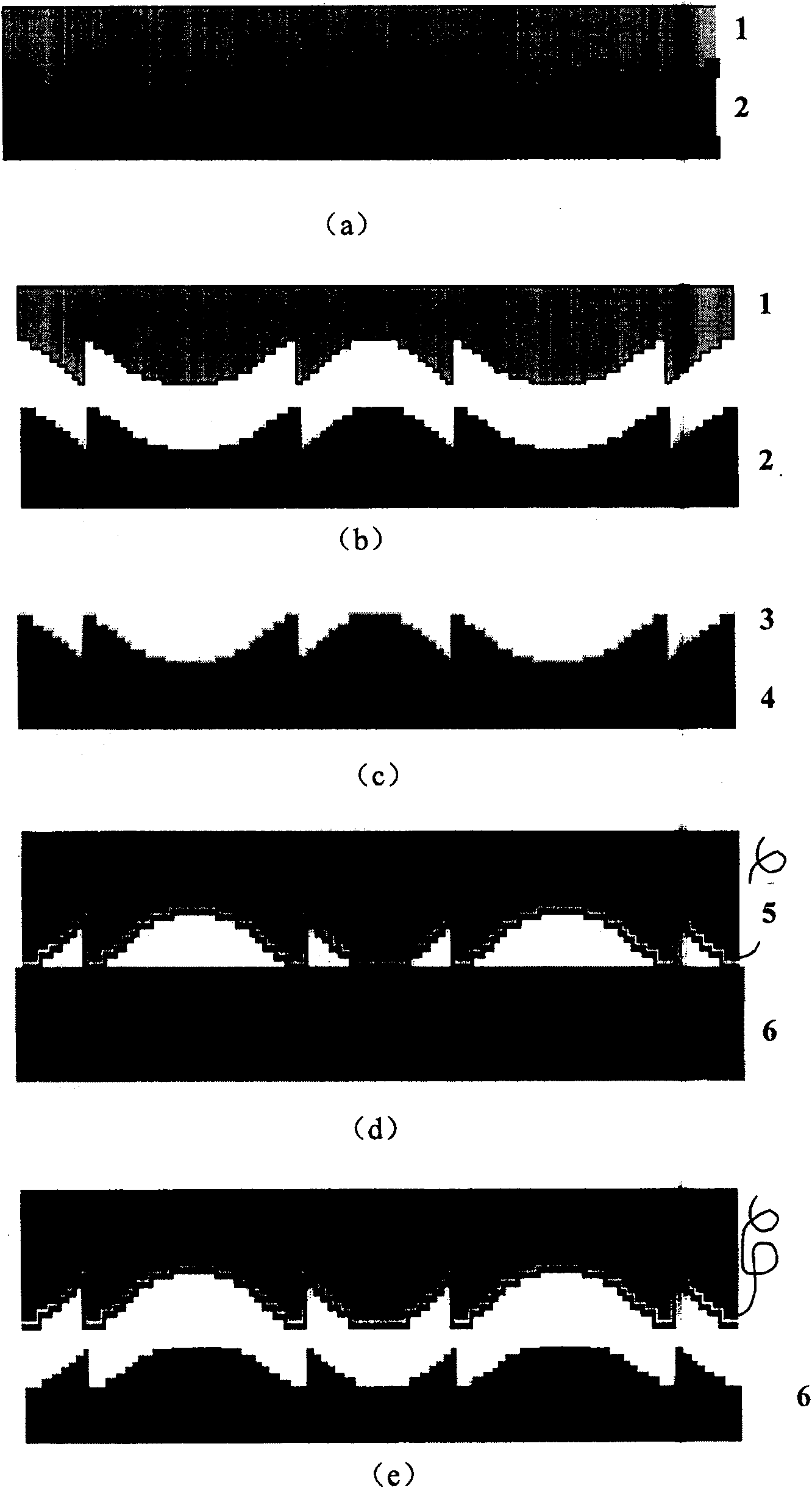
[0036] figure 1 A schematic diagram of the processing technology of Example 1 of the present invention is given.
[0037] figure 1 a is the hot embossing process, the polymer material is PMMA 2 (polymethyl methacrylate) and the quartz optical element master 1 is placed in the hot embossing device, the selected glass transition temperature (T g ) temperature is 100°C. PMMA 2 has a thickness of 1mm and an area of 2cm 2 ,use figure 2 The shown hot embossing device is heated up to the glass transition temperature (T g ) above (generally controlled at 135°C), and then apply a pressure of 4 to 10 MPa for replication.
[0038] figure 1 B is the demoulding and separation process after hot pressing replication. After the hot pressed PMMA sheet 2 is separated from the quartz optical element master plate 1, the PMMA sheet 2 also needs to be degreased. 3 PO 4 50g / L+Na 2 CO 3 25g / L+NaOH 20g / L for degreasing treatment, the deoiling temperature is 85°C, and the time is 2.5h.
...
Embodiment 2-6
[0047] The specific operation steps of Examples 2-6 are the same as those of Example 1, and the specific composition of the solution is shown in Table 1, wherein the etching effect "+" is good.
[0048] Table 1
[0049] Example
PUM
| Property | Measurement | Unit |
|---|---|---|
| thickness | aaaaa | aaaaa |
| thickness | aaaaa | aaaaa |
| thickness | aaaaa | aaaaa |
Abstract
Description
Claims
Application Information