Ultra-thin solar silicon slice and its cutting technology

A technology of solar-grade silicon wafers and cutting technology, which is applied in the field of solar cells, can solve the problems of easily damaged round edges of cylinders, failure to recycle and reduce the pass rate of finished products, etc., to achieve economic benefits, increase output, and improve The effect of production efficiency

Inactive Publication Date: 2009-12-02
江苏有则创投集团有限公司
View PDF4 Cites 0 Cited by
  • Summary
  • Abstract
  • Description
  • Claims
  • Application Information

AI Technical Summary

Problems solved by technology

This cross-sectional solar-grade silicon wafer has the following disadvantages: First, the waste chips from the rolling process are powdery, which float in the air and pollute the environment, and cannot be recycled and reused; second, the rolling process easily damages the round edges of the cylinder , Quality problems such as chipping and bursting occur, thereby reducing the qualified rate of finished products

Method used


Image

  • Ultra-thin solar silicon slice and its cutting technology
  • Ultra-thin solar silicon slice and its cutting technology
  • Ultra-thin solar silicon slice and its cutting technology

Examples


Embodiment 1

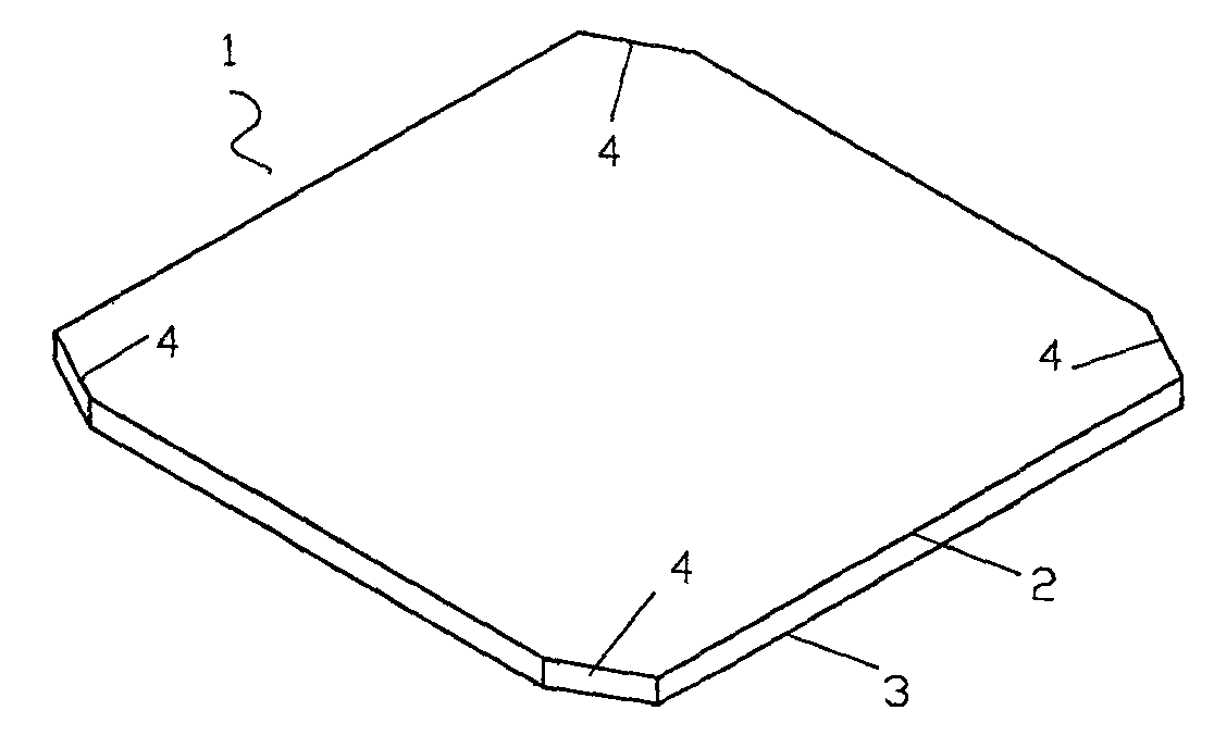
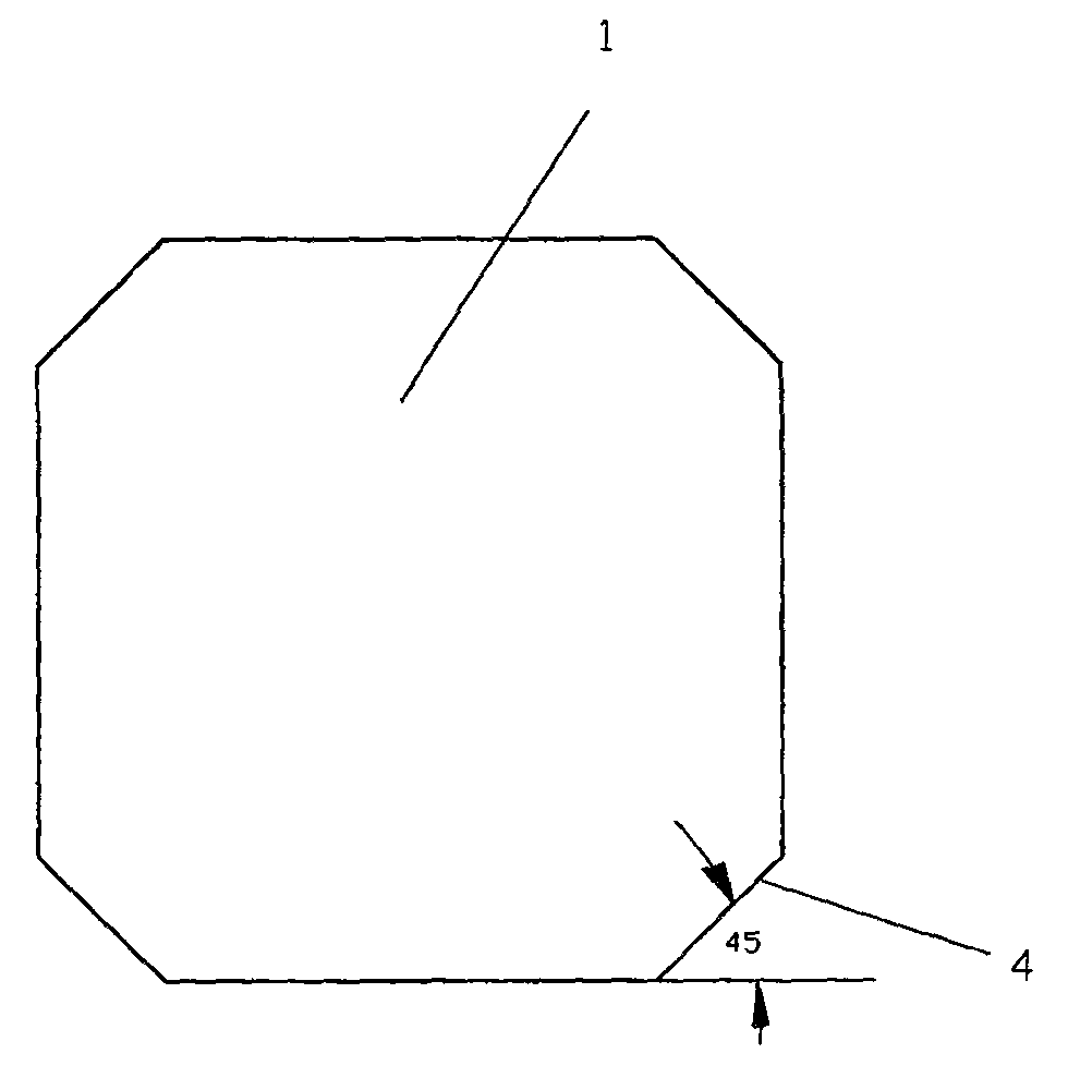
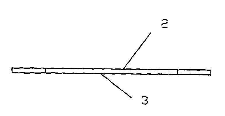
[0014] See figure 1 , figure 2 and image 3 Shown are the perspective view, front view and top view of the ultra-thin solar grade silicon wafer. This embodiment is an ultra-thin solar-grade silicon wafer with a specification of 125mm×125mm, which is composed of upper and lower parallel planes 2 and 3, and its four corners 4 are four identical 45° chamfers. The distance between the upper and lower planes 2 and 3 is within the range of 165 μm-195 μm, the degree of warpage is less than 75 μm, and the surface is smooth, smooth and free from blemishes.

[0015] See Figure 4 Shown is a schematic diagram of the ultra-thin solar-grade silicon wafer cutting process.

[0016] The processing method of this embodiment is to use a silicon crystal ingot squarer to square A = Φ156mm silicon single wafer bar twice and chamfer it twice, and cut it into a square with a cross section of C = 125mm and four identical corners. An octagonal square cylinder with a 45° chamfer and a distance ac...

Embodiment 2

[0022] Embodiment 2 is an ultra-thin solar-grade silicon wafer with a specification of 156mmX156mm. Its main body 1 is composed of upper and lower parallel planes 2 and 3, and its four corners 4 are four identical 45° chamfers. The distance between the upper and lower planes 2 and 3 is within the range of 165 μm-195 μm, the degree of warpage is less than 75 μm, and the surface is smooth, smooth and free from blemishes.

[0023] The processing method of this embodiment is to use a silicon crystal ingot squarer to square A=Φ203mm silicon single wafer rod twice and chamfer it twice, and cut it into a square with a cross section of C=156mm and four identical four corners. 45° chamfer, octagonal square cylinder with distance across sides B=195mm. The cutting process parameters for squaring and chamfering are steel wire speed 11 m / s and workpiece speed 700 microns / min.

[0024] After ultrasonic cleaning and high-purity nitrogen blow-dry the square silicon rod after prescription, st...


PUM

PropertyMeasurementUnit
thicknessaaaaaaaaaa
densityaaaaaaaaaa
thicknessaaaaaaaaaa

Abstract

The invention relates to an ultra-thin sun energy level silicon chip and cutting technology thereof which belongs to the solar cell field. The body of the ultra-thin sun energy level silicon chip is the square slice composed of upper and lower planes in parallel, the foursquare of the square slice is four same chamfer angle of 45 DEG. The distance of the upper and lower planes is in the scope of 165-195 um, the angularity is less than 75 um, and the surface of the plane is bright, flat and flawless. The ultra-thin sun energy level silicon chip cutting technology adopts a silicon wafer stick excavator to directly cut silicon wafer stick into octagonal square cylinder whose cross-section is square and foursquare is the same chamfer angle of 45 DEG, the cutting excess stock is lump which can be reused by scrap. It also adopts optimized cutting technology to cut into the ultra-thin sun energy level silicon chip on the multi-thread cutting machine so as to guarantee the manufacturing quality of the ultra-thin sun energy level silicon chip, improve productivity, and reduce the manufacturing cost of ultra-thin sun energy level silicon chip.

Description

technical field [0001] The invention relates to an ultra-thin solar grade silicon wafer and a cutting process thereof, belonging to the field of solar cells. Background technique [0002] At present, silicon wafers for solar cells are cut from single crystal round silicon rods. Domestic silicon crystal materials are scarce and expensive. With the widespread application of renewable energy, the market demand for solar-grade silicon wafers is increasing. The traditional solar silicon wafers that are commonly used in the world are square sheets with rounded corners and a thickness of more than 200 μm. The processing procedure for this solar-grade silicon wafer is: first cut the round silicon rod into a square section. , The four corners are left with the cylinder of the rounded edge of the billet, and then the rounded edge of the billet is tumbled to the standard fillet size with a grinding wheel, and the grinding amount is about 2mm-4mm. This cross-sectional solar-grade sili...

Claims


Application Information

Patent Timeline
Patent Type & Authority Patents(China)
IPC IPC(8): H01L31/0352H01L31/18B28D5/00
CPCY02P70/50
Inventor 吴伟忠毛和璜李云霞
Owner 江苏有则创投集团有限公司
Why Eureka
Try Eureka