Thin film transistor array base and its pixel structure

A technology of thin film transistors and array substrates, which is applied in the field of active element array substrates, can solve problems such as resistance and capacitance hysteresis, color shift and insufficient color saturation, and achieve the effect of improving resistance and capacitance hysteresis and enhancing display effects

Active Publication Date: 2007-07-25
AU OPTRONICS CORP
View PDF0 Cites 13 Cited by
  • Summary
  • Abstract
  • Description
  • Claims
  • Application Information

AI Technical Summary

Problems solved by technology

[0007] The purpose of the present invention is to provide a thin film transistor array substrate to solve the problem of resistance and capacitance hysteresis caused by the large size of the liquid crystal display panel
[0008] Another object of the present invention is to provide a pixel structure to solve the problems of color shift and insufficient color saturation at different viewing angles

Method used


Image

  • Thin film transistor array base and its pixel structure
  • Thin film transistor array base and its pixel structure
  • Thin film transistor array base and its pixel structure

Examples


Embodiment Construction

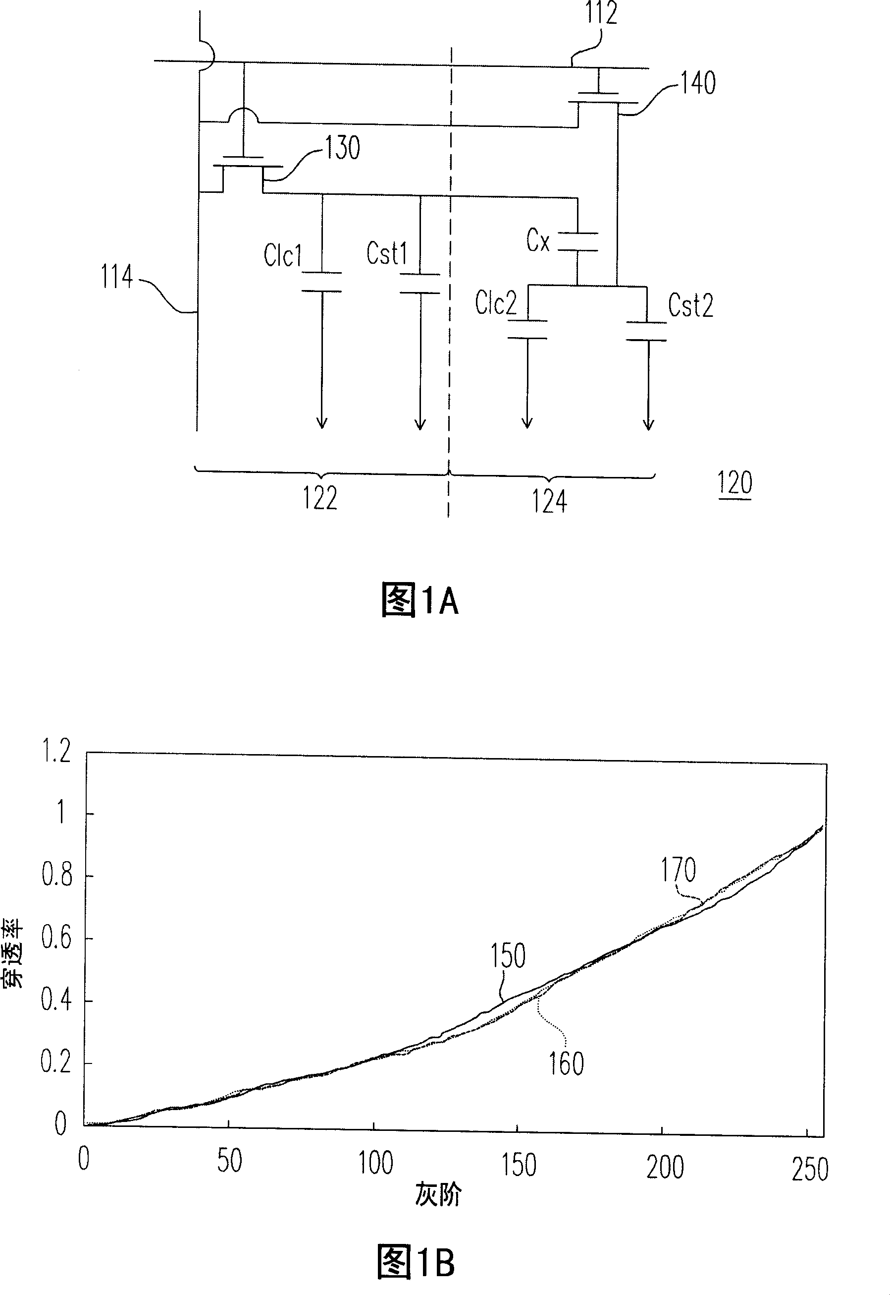
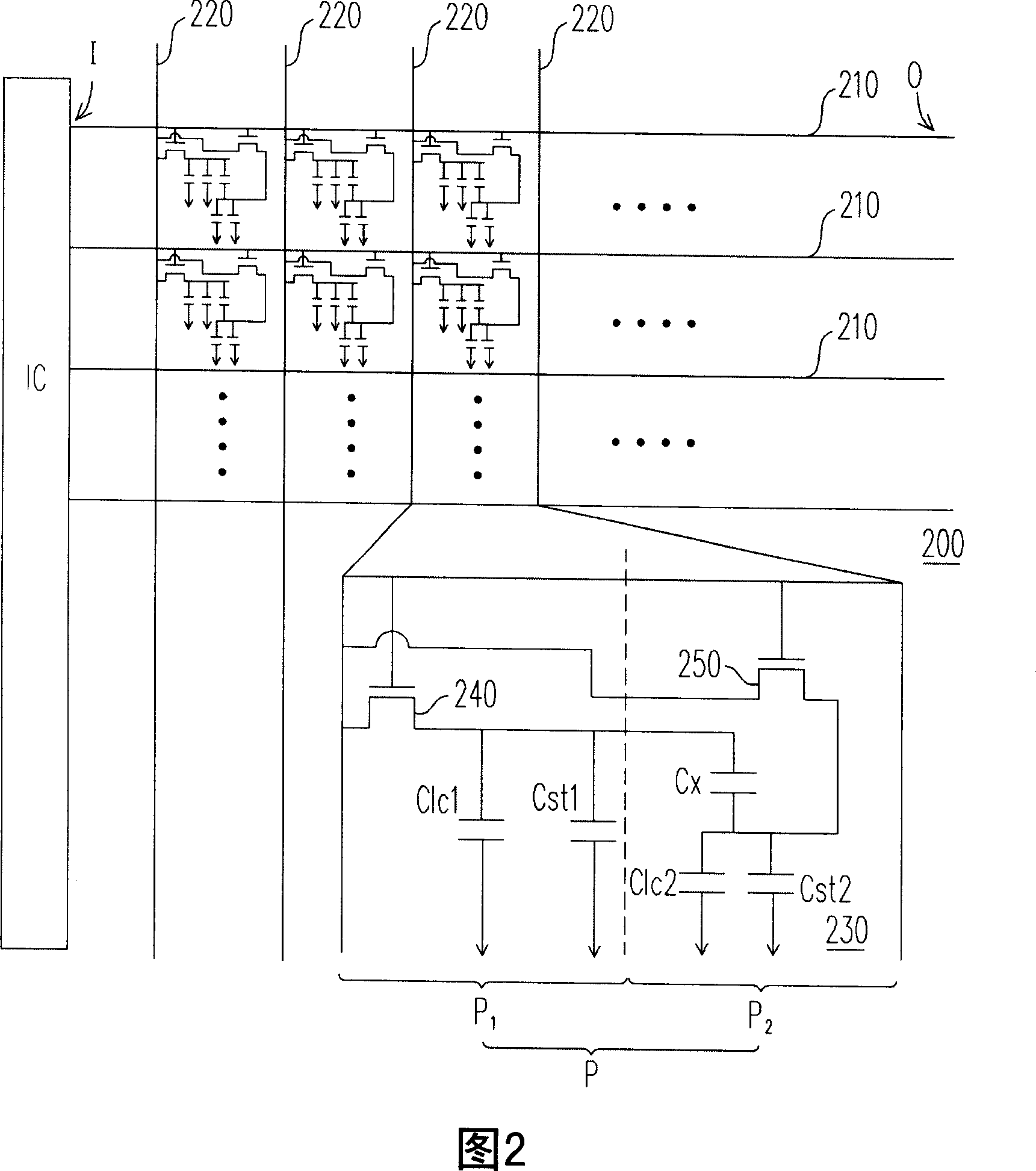
[0061] Generally speaking, in order to improve the resistance-capacitance hysteresis in the liquid crystal display panel, it is necessary to make each thin film transistor on the same scanning line in the thin film transistor array substrate have the same charge and discharge performance. Therefore, the present invention proposes a design of a thin film transistor array substrate. By changing the width and length of the channel layer in the thin film transistor, the thin film transistor far away from the input terminal of the driving signal has a larger W / L ratio, and the thin film transistor close to the input terminal of the driving signal has a larger W / L ratio. Transistors have a small W / L ratio. In this case, the charging and discharging performances of the thin film transistors on the same scan line can be approximately the same.

[0062] FIG. 2 is a schematic diagram of a thin film transistor array substrate according to a preferred embodiment of the present invention. ...


PUM


Abstract

The base plate of thin film transistor (TFT) array includes a substrate, multiple pieces of scanning wiring collocated on the substrate, multiple pieces of data wiring collocated on the substrate, and multiple pixel structures. Possessing inputting ends and tail ends of drive signal, the multiple pieces of scanning wiring and data wiring divide the substrate into multiple pixel areas. Each pixel area includes the pixel area for the first time (PAF) and the pixel area for the second time (PFS). Being collocated in pixel areas, pixel structure is driven by scanning wiring and data wiring. In a pixel area affiliated with, pixel structure includes first TFT corresponding to PAF, and second TFT corresponding to PAS. On the same scanning wiring, ratio between width and length of channel of the second TFT is crescent from inputting end of the drive signal to tail end in order to solve issues of delay of resistance capacitance, color deflection, and deficient color saturation.

Description

technical field [0001] The invention relates to an active element array substrate, in particular to a thin film transistor array substrate of a liquid crystal display panel and a pixel structure thereof. Background technique [0002] As liquid crystal displays continue to develop toward large-size display specifications, in order to overcome the viewing angle problem under large-size displays, the wide viewing angle technology of liquid crystal display panels must also continue to improve and break through. Among them, a multi-domain vertical alignment (MVA) liquid crystal display panel is a common wide viewing angle technology at present. [0003] Generally speaking, the multi-domain vertical alignment type liquid crystal display panel utilizes the design of the alignment structure, so that the liquid crystal layer in the same pixel region is divided into multiple different regions. Wherein, the liquid crystal molecules in different regions have different alignment directi...

Claims


Application Information

Patent Timeline
Patent Type & Authority Applications(China)
IPC IPC(8): H01L27/12H01L29/786G02F1/1362
Inventor 曹正翰黄乙白张庭瑞
Owner AU OPTRONICS CORP
Why Eureka
Try Eureka