Metallic mold for nano-imprint, forming method of nano-pattern, and resin molding

A technology of nano-imprinting and nano-patterning, which is applied in the field of resin molding to achieve the effect of high adhesion

Inactive Publication Date: 2007-08-08
堀胜 +2
View PDF1 Cites 3 Cited by
  • Summary
  • Abstract
  • Description
  • Claims
  • Application Information

AI Technical Summary

Problems solved by technology

In addition, significant investments must be made in the equipm

Method used


Image

  • Metallic mold for nano-imprint, forming method of nano-pattern, and resin molding
  • Metallic mold for nano-imprint, forming method of nano-pattern, and resin molding
  • Metallic mold for nano-imprint, forming method of nano-pattern, and resin molding

Examples


Embodiment approach 1

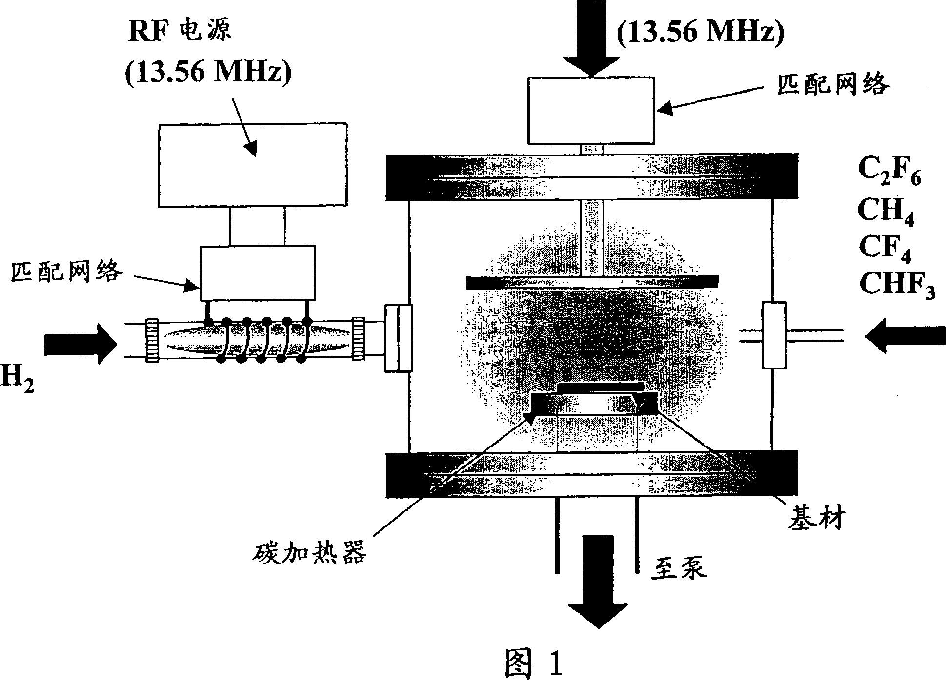
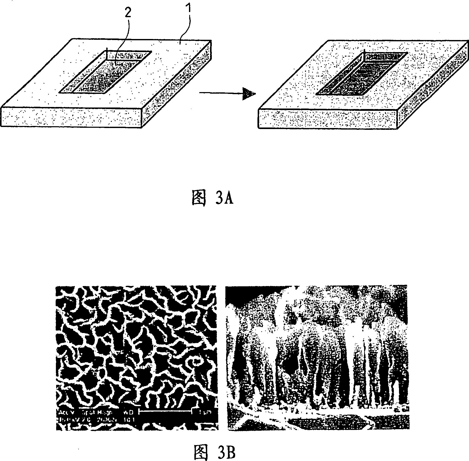
[0041] Mold structures with CNW patterned stencils were prepared. In this embodiment, the convex portion of the CNW corresponds to the concave portion of the molded article. Referring to FIG. 6 , CNWs ( 1 ) were produced on a substrate for producing CNWs under the conditions described above for the method of producing CNWs. This is followed by nickel plating (2) on the surface of the CNW. Plating methods may involve substances other than nickel. Then, the CNWs are peeled off from the substrate (3). Alternatively, the CNW can be partially combusted. Finally, fix the CNWs onto the mold surface.

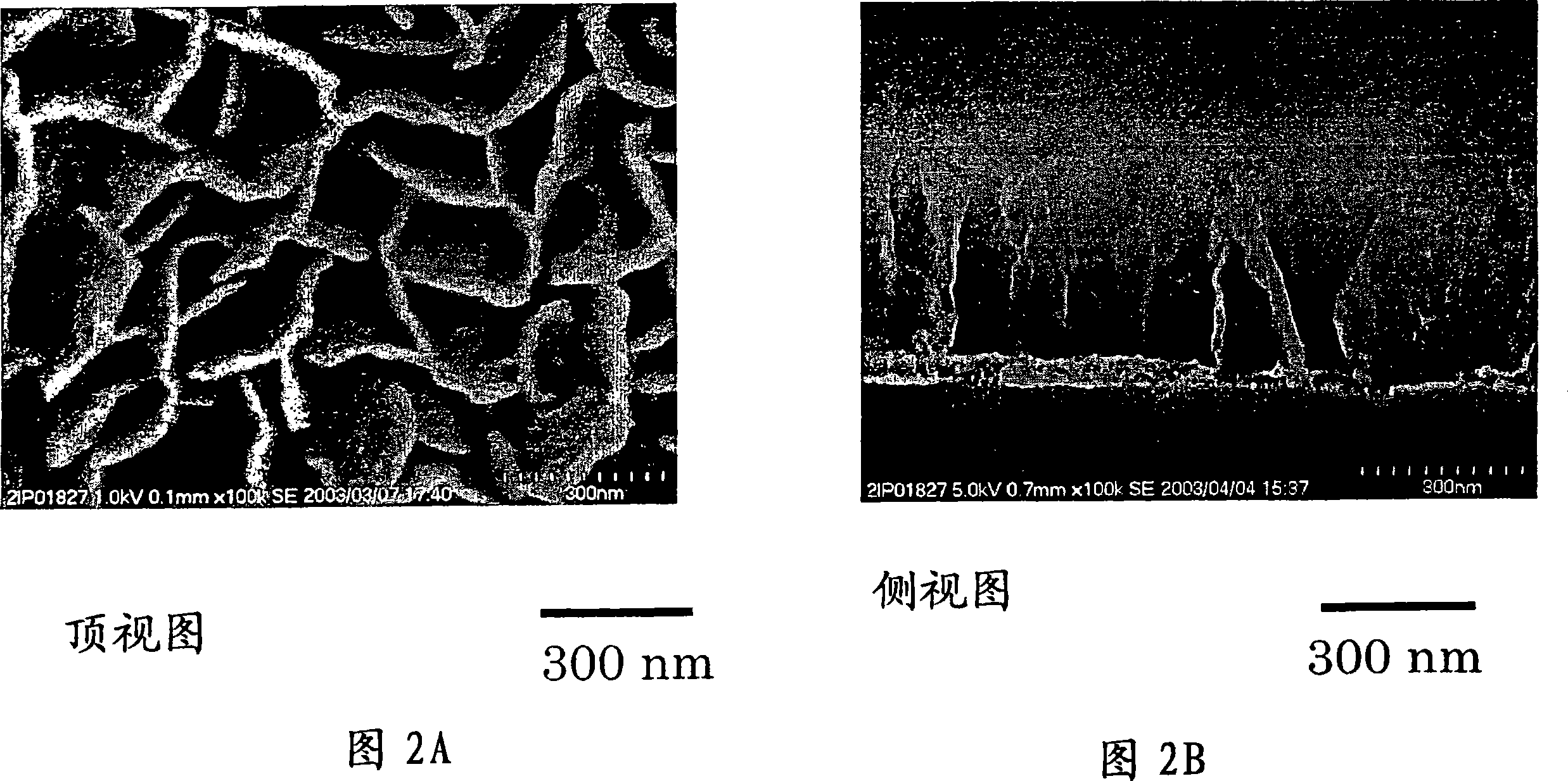
[0042] In this embodiment, as shown in the conceptual image in the figure, the white portion of the SEM image of CNW corresponds to the convex portion of the resin molded article.

Embodiment approach 2

[0044] As shown schematically in Figure 7, a mold structure with a reverse CNW patterned mold was prepared. In this embodiment, the raised portion of the CNW corresponds directly to the raised portion of the molded article. First, CNWs (1) were produced on a substrate for producing CNWs under the conditions described above in the method of forming CNWs. Figure 8 shows the SEM image of the CNW surface before the electroless nickel plating method. Then, a Ni plating layer (2) is provided to the surface of the CNW. Figure 9 shows the SEM image of the CNW surface after the electroless nickel plating method. Plating methods may involve substances other than nickel. The CNWs are then peeled off from the substrate (3). Figure 10 shows a SEM image of the surface on the CNW removed side after removing the CNWs by firing. From Figure 10, it is clear that there is an inverse pattern of CNWs. The remaining CNWs were fired at 700°C in air. Finally, fix the CNW onto the mold surface ...


PUM


Abstract

Releasability of a mold and a resin layer during nanoimprinting is improved, thereby improving the durability of the mold. A nanoimprint mold for resin molding comprising a carbon nanowall layer provided on the surface thereof, a method of forming a nanopattern using the mold, and a resin-molded product obtained by the method.

Description

technical field [0001] The present invention relates to a nanoimprint mold, a method of forming a nanopattern, and a resin molded article obtained by the method of forming a nanopattern. Background technique [0002] The only way to achieve miniature production with satisfactory precision and mass productivity has long been considered to be photolithography. However, since photolithography uses propagated light, it suffers from diffraction limit. For example, in an exposure apparatus having a light source emitting g-line (436 nm) or i-line (365 nm), the maximum resolving power is 0.3 μm to 0.5 μm. In order to improve the resolution, the wavelength of the exposure light source must be made shorter. For this reason, in order to achieve higher densities in LSIs or the like, research has been conducted on excimer laser steppers using KrF (248 nm), ArF (193 nm), and F2 (157 nm). EUV (including X-rays of tens of nanometers) is also being investigated as a related future technol...

Claims


Application Information

Patent Timeline
IPC IPC(8): G03F7/00B82B3/00C23C16/26
Inventor 堀胜平松美根男加纳浩之杉山徹片山幸久吉田怜
Owner 堀胜
Why Eureka
Try Eureka