
Automatic detecting system and method for planar substrate

An automatic detection, flat substrate technology, applied in the defect system field, can solve the problems of small size, large substrate area, short detection time, etc., and achieve the effect of reducing weight and volume, high response speed and high sensitivity

Active Publication Date: 2007-08-22
ZHAOQING ZHONGDAO OPTOELECTRONICS EQUIP CORP
View PDF0 Cites 60 Cited by
  • Summary
  • Abstract
  • Description
  • Claims
  • Application Information

AI Technical Summary

Problems solved by technology

The inspection of flat-panel displays faces special technical challenges because the substrate is made of transparent materials, the lines on the surface have a multi-layer structure, the imprinted patterns are dense, the size of the defects is very small (on the order of microns), the area of ​​the substrate is too large, and the inspection time very short

Method used


Image

  • Automatic detecting system and method for planar substrate
  • Automatic detecting system and method for planar substrate
  • Automatic detecting system and method for planar substrate

Examples


Embodiment Construction

[0026] The following description provides numerous details to describe and understand an example of a detection system and method. Those skilled in the art will recognize that the examples can be practiced without one or more of the details, or with additional elements. In other words, well-known structures and operations are not shown or described in detail.

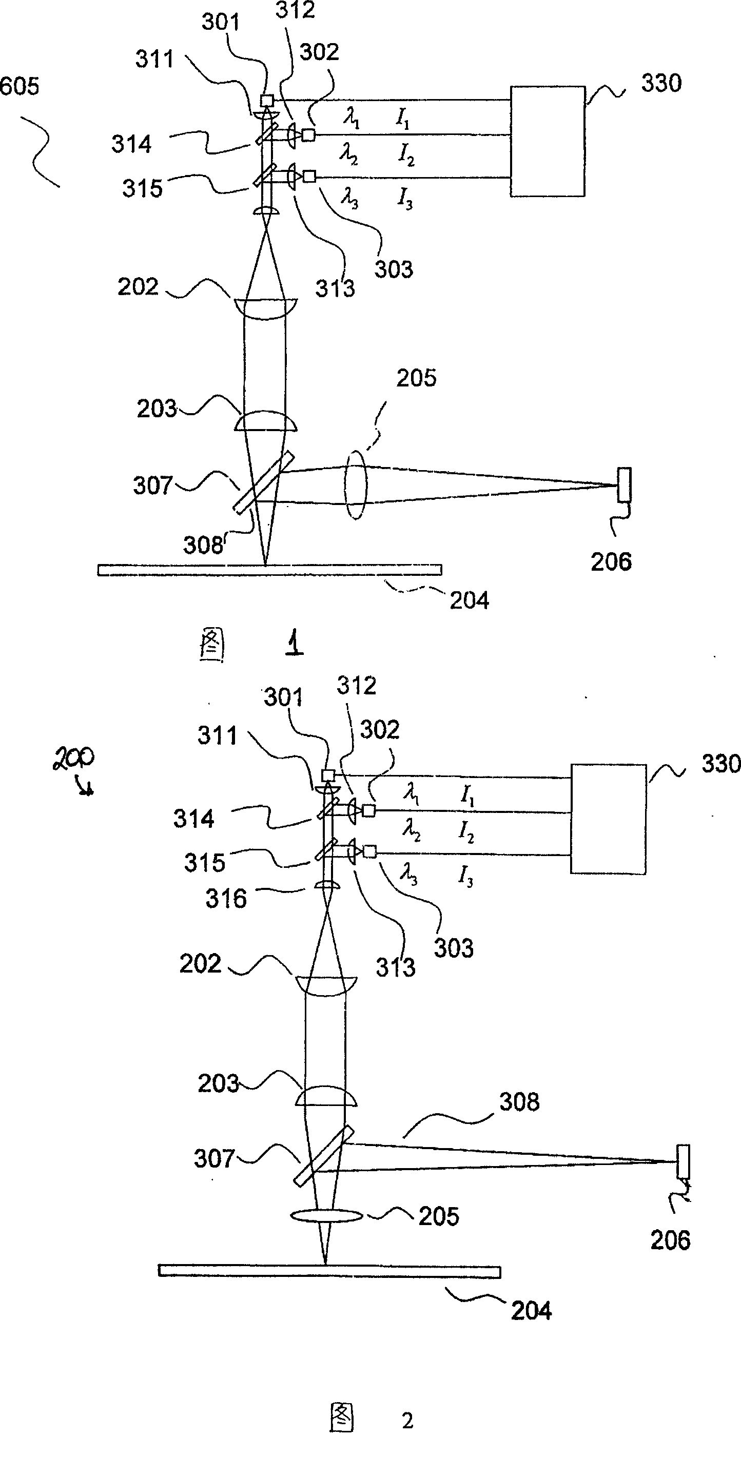
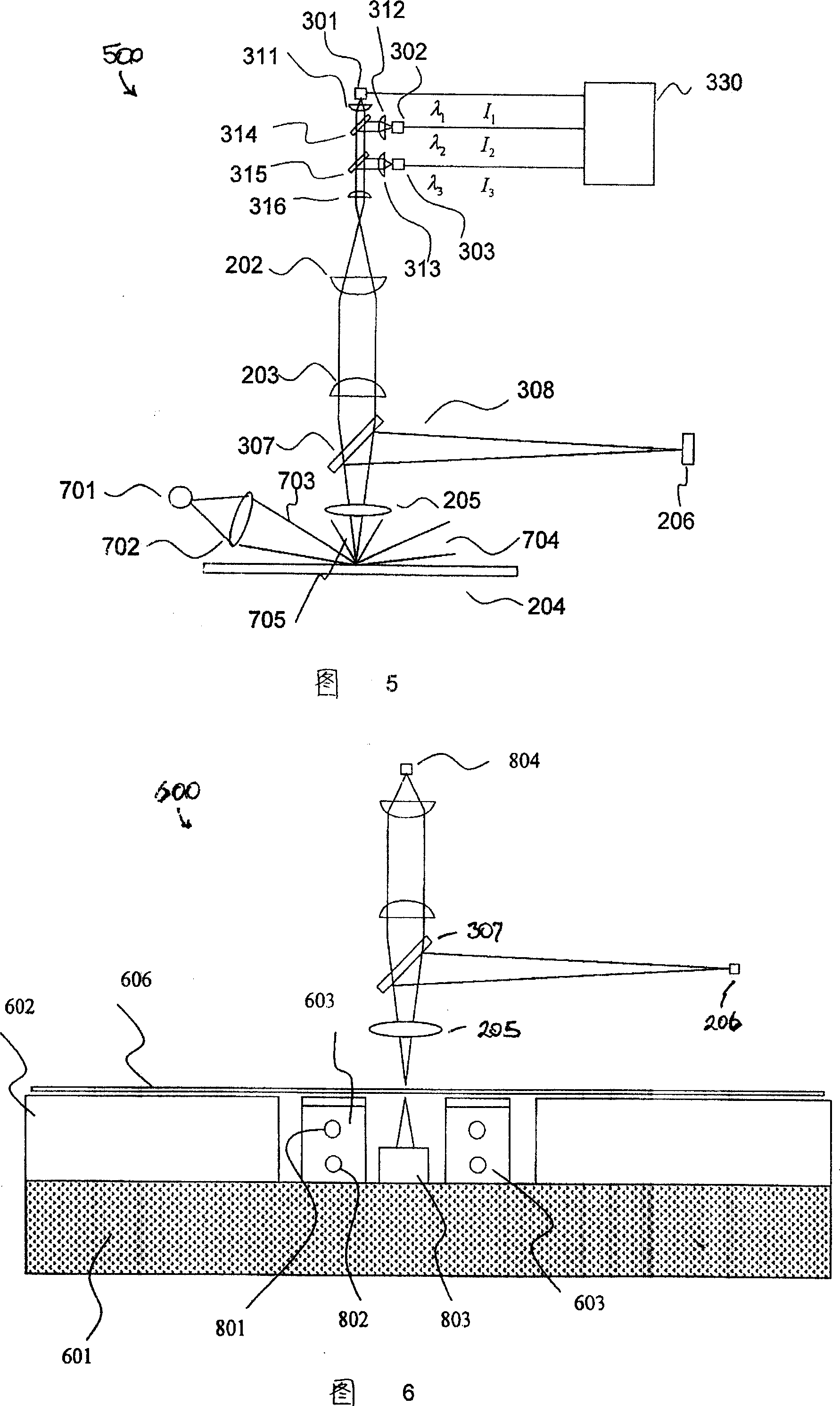
[0027] FIG. 1 is an example block diagram of an optical module 605 of an automated optical inspection system. The optical module 605 is used to detect the substrate and perform defect judgment and location. This goal can be achieved by detecting defect signals proportional to the product of incident light intensity and integration time. The optical module 605 includes a plurality of LED light sources, and each LED light source emits light of different wavelengths to be incident on the planar substrate to be inspected. Although in this example the optical module 605 has three LED light sources producing three wavelengt...


PUM


Abstract

The invention discloses an automatic detecting system and method of flat base plate, which contains an optical module. The optical module has illuminating module and lens array leading beam to part of base plate. Lens array contains a Fresnel lens and optical module contains a camera. The camera has time delay integral (TDI) sensor, which receives reflected light producing by illuminating source and base plate. Telecentric imaging lens leads reflected light from base plate to camera. Illuminating module has a controller connected with a source containing multi-group LED (each LED can radiate light with different wavelength) and the controller control each LED independently. The invention can analyze large-scale flat base plate quickly, has high sensitivity and can provide high-resolution picture.

Description

technical field [0001] The invention belongs to the field of detection systems, in particular to a system and method for detecting defects of imprinted patterns on a plane substrate. technical background [0002] Defect monitoring is a critical step in the production and processing of large substrates such as flat panel displays. Flat-panel displays are mainly used in personal notebook computers, computer flat-panel displays, mobile phone and digital instrument displays, car guidance systems, cameras, projection TVs and LCD TVs, as well as large and small displays on many instruments. A flat panel display is composed of two transparent substrates (usually glass). A control circuit and an optical color filter are printed on the substrate, and liquid crystals are filled between the two substrates. The processing of flat panel display products is very complicated and must be carried out in an ultra-clean environment, otherwise it is easily affected by various defects in the p...

Claims


Application Information

Patent Timeline
IPC IPC(8): G01N21/956G01R31/309
CPCG01N21/95607G02B3/08G01N21/8851G01N2021/5957G01N2021/8816H04N25/00
Inventor 严征李波陈维华杨铁成李宁高剑波
Owner ZHAOQING ZHONGDAO OPTOELECTRONICS EQUIP CORP
Features
  • Generate Ideas
  • Intellectual Property
  • Life Sciences
  • Materials
  • Tech Scout
  • Unparalleled Data Quality
  • Higher Quality Content
  • 60% Fewer Hallucinations
Learn More