Liquid crystal display panel
A liquid crystal display panel and substrate technology, applied in static indicators, nonlinear optics, instruments, etc., can solve the problems of liquid crystal display panel aperture ratio drop, dark state light leakage, liquid crystal display panel aperture ratio limitation, etc., to improve the dark state Effects of light leakage, increased aperture ratio, optimum aperture ratio, and contrast
- Summary
- Abstract
- Description
- Claims
- Application Information
AI Technical Summary
Problems solved by technology
Method used
Image

Examples
no. 1 example
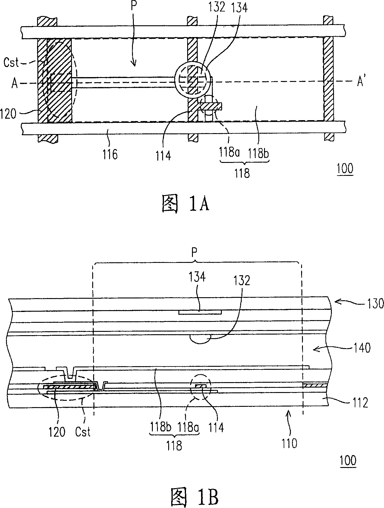
[0057] 1A and 1B are respectively a top view and a schematic cross-sectional view of a liquid crystal display panel according to a first embodiment of the present invention. Please refer to FIG. 1A and FIG. 1B at the same time. The liquid crystal display panel 100 of this embodiment includes an active device array substrate 110 , an opposite substrate 130 and a liquid crystal layer 140 . The active device array substrate 110 includes a substrate 112 , scan lines 114 , data lines 116 and pixel units 118 disposed on the substrate 112 . The pixel unit 118 is electrically connected to the corresponding scan line 114 and the data line 116 , and the pixel unit 118 straddles the two sides of the corresponding scan line 114 . Alignment protrusions 132 are formed on the opposite substrate 130 , and the alignment protrusions 132 are located above the scan lines 114 . The liquid crystal layer 140 is disposed between the opposite substrate 130 and the active device array substrate 110 . ...
no. 2 example
[0062] In order to disclose the spirit of the present invention in more detail, the structure of the liquid crystal display panel of the second embodiment of the present invention is proposed here.
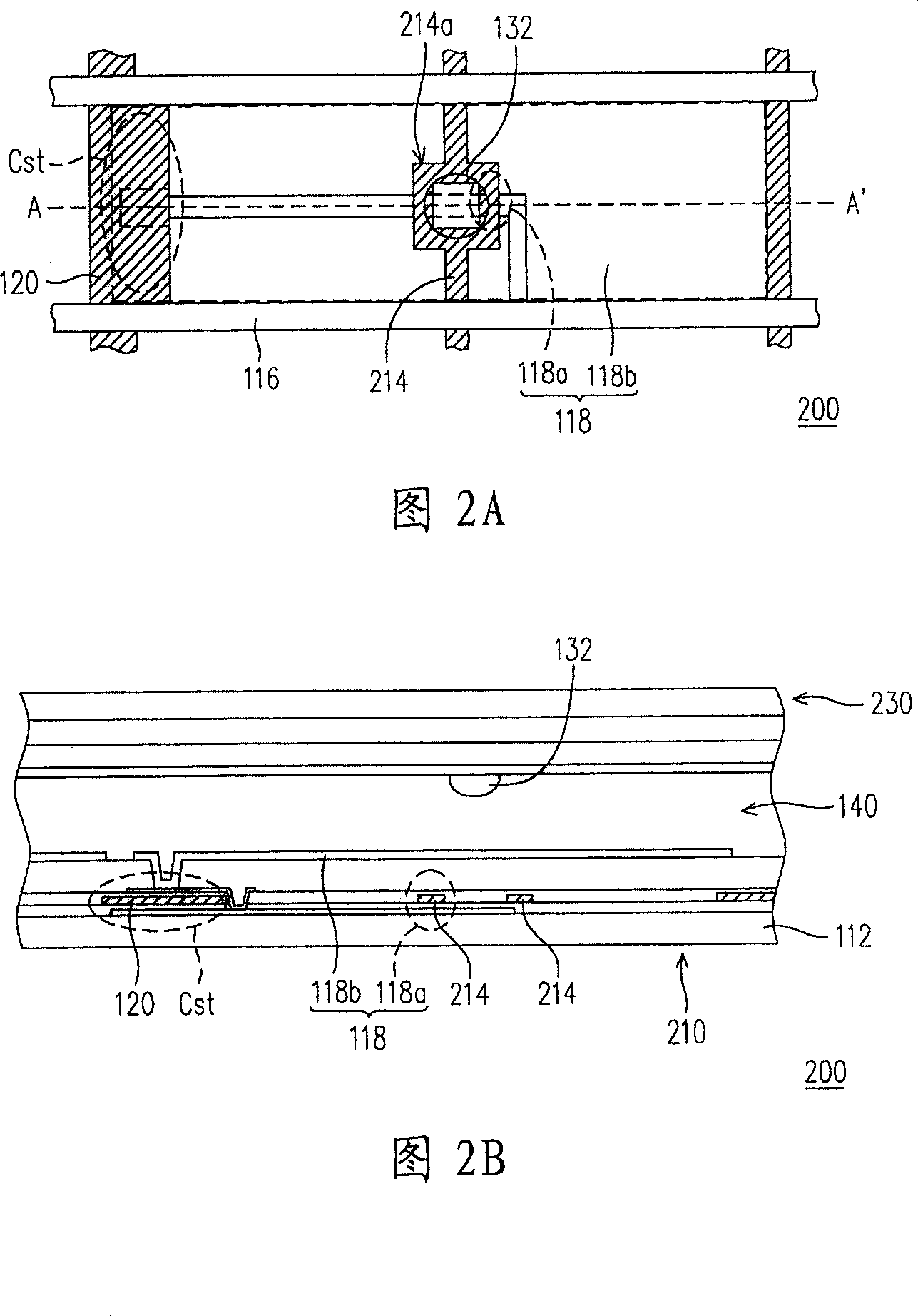
[0063] FIG. 2A is a schematic top view of a liquid crystal display panel according to a second embodiment of the present invention, and FIG. 2B is a schematic cross-sectional view along line AA' of FIG. 2A . Please refer to FIG. 2A and FIG. 2B at the same time. The liquid crystal display panel 200 of this embodiment is similar to the liquid crystal display panel 100 of the first embodiment, so the same component symbols represent the same meanings, which will not be repeated here. The difference between the two is that there is no need to configure the black matrix 134 for shielding light on the opposite substrate 230 of the liquid crystal display panel 200. In this embodiment, the scanning line 214 on the active device array substrate 210 is designed to have a ring-shaped frame pa...
no. 3 example
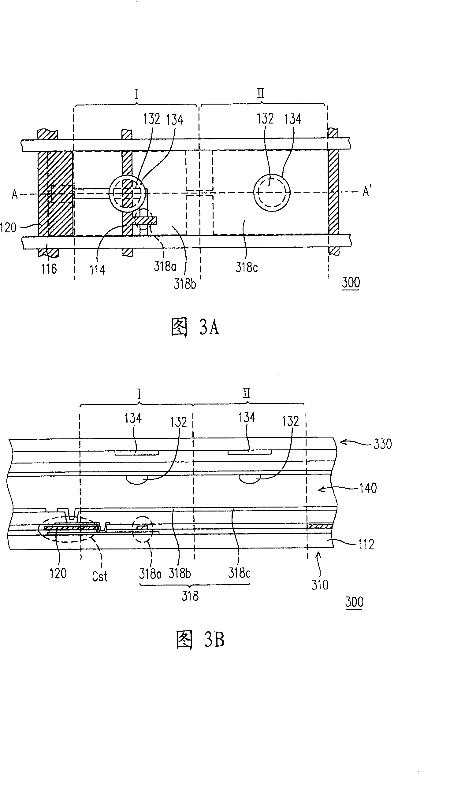
[0066] FIG. 3A is a schematic top view of a liquid crystal display panel according to a third embodiment of the present invention, and FIG. 3B is a schematic cross-sectional view along line AA' of FIG. 3A . Please refer to FIG. 3A and FIG. 3B at the same time. The liquid crystal display panel 300 of this embodiment is similar to the liquid crystal display panel 100, but the main difference between the two is that the pixel unit 318 of the liquid crystal display panel 300 has a first area I and a second area II. . Wherein, for example, the alignment protrusions 132 are respectively located above the first region I and above the second region II. In addition, the pixel unit 318 has, for example, a first pixel electrode 318b and a second pixel electrode 318c, and the first pixel electrode 318b and the second pixel electrode 318c are respectively located in the first region I and the second region II.
[0067] In this embodiment, both the first pixel electrode 318b and the second...
PUM
 Abstract
Description
Claims
Application Information
 - R&D
- Intellectual Property
- Life Sciences
- Materials
- Tech Scout
- Unparalleled Data Quality
- Higher Quality Content
- 60% Fewer Hallucinations
Browse by: Latest US Patents, China's latest patents, Technical Efficacy Thesaurus, Application Domain, Technology Topic, Popular Technical Reports.
© 2025 PatSnap. All rights reserved.Legal|Privacy policy|Modern Slavery Act Transparency Statement|Sitemap|About US| Contact US: help@patsnap.com