Analog source electrode driver output voltage compensating device and method thereof
A technology of output voltage and compensation device, used in instruments, static indicators, etc., can solve problems such as the drop in grade grayscale performance, and achieve the effects of improving picture quality, improving block defects, and eliminating output voltage fluctuations.
- Summary
- Abstract
- Description
- Claims
- Application Information
AI Technical Summary
Problems solved by technology
Method used
Image
Examples
Embodiment Construction
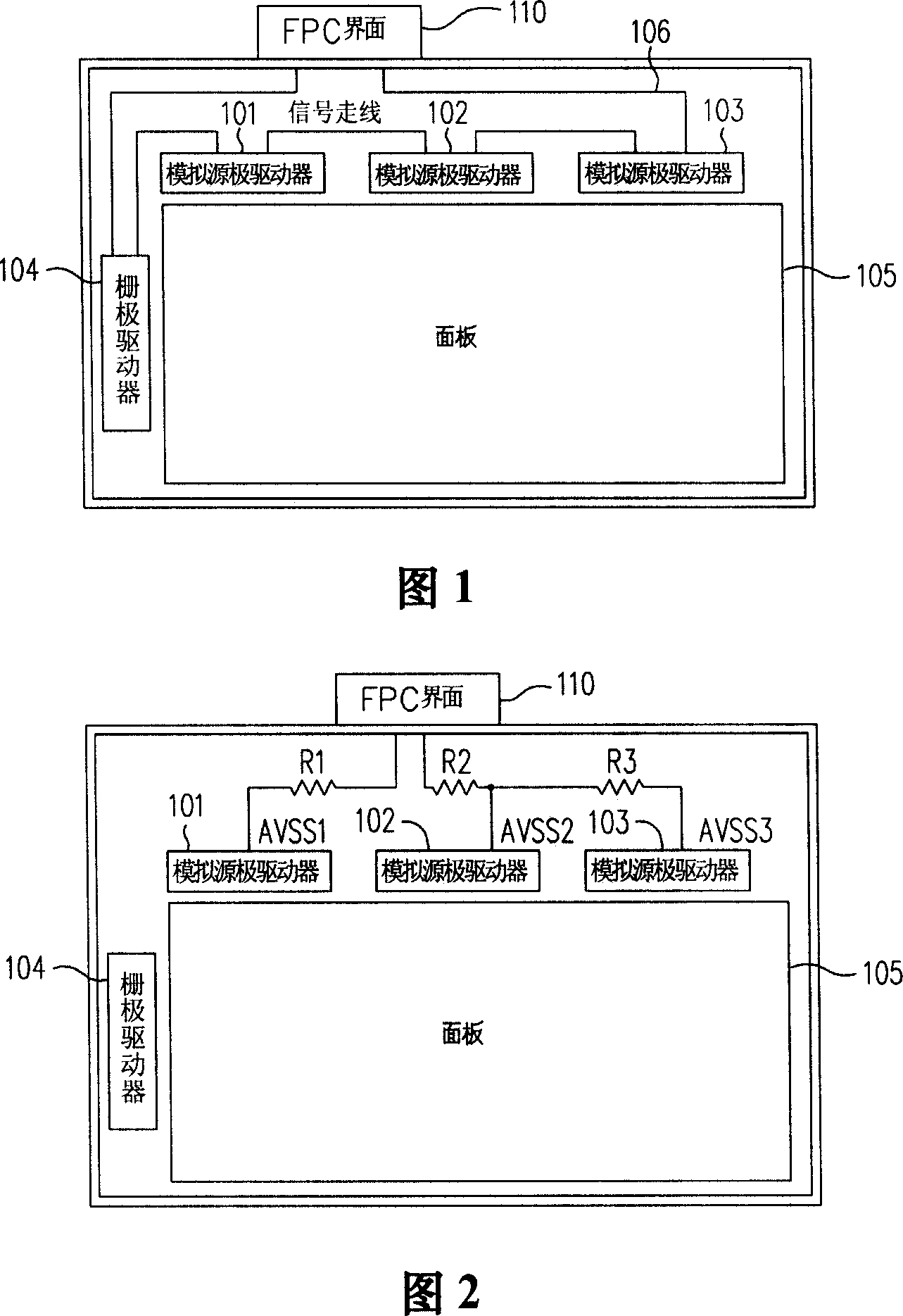
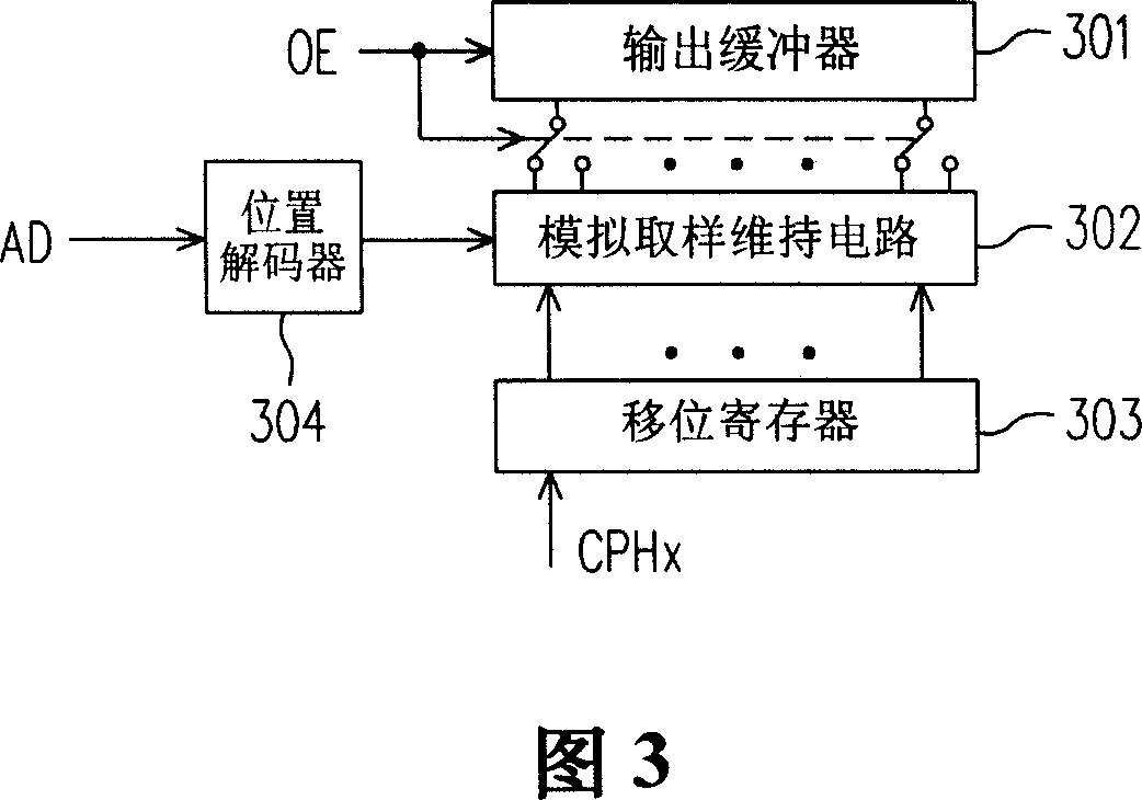
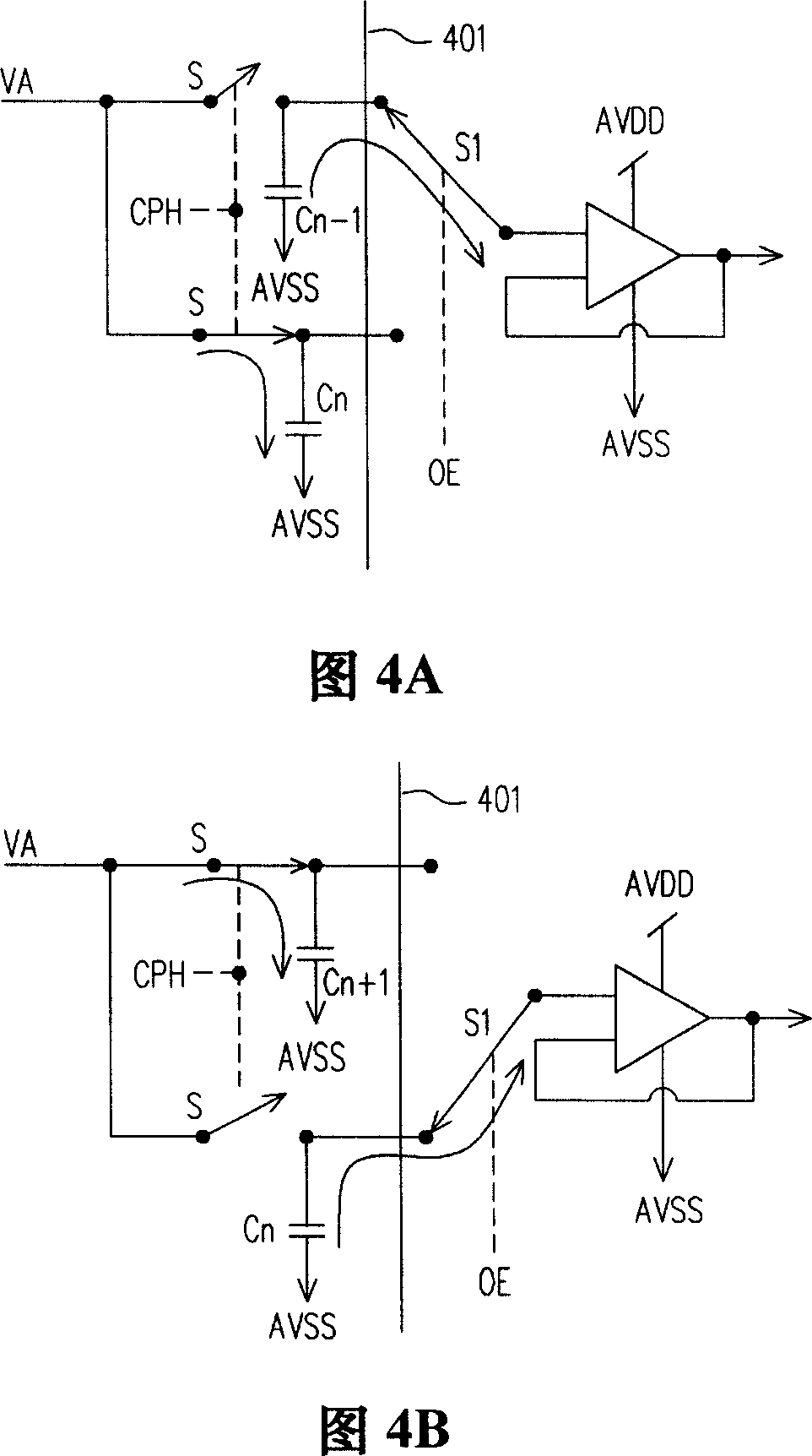
[0045] FIG. 6 is a structural diagram of an analog liquid crystal panel driving system according to an embodiment of the present invention, including a parameter selector (parameter selector) 611, a phase locked loop circuit (phase locked loop) 612, a video decoder (video decoder) 613, and a timing controller. (timing controller) 614 , DC / DC converter (DC / DC converter) 616 , and panel module 615 with analog source drivers 621 - 623 , gate driver 624 and panel 625 with output voltage compensation device 75 . The video decoder 613 is used for data decoding of the input video signal VS, and outputs analog data AD. The timing controller 614 generates the source control signal CS required by the analog source drivers 621 - 623 and the gate control signal CG required by the gate driver 624 . The parameter selector 611 provides the video decoder 613 with decoding parameters required by different video systems. The PLL circuit 612 provides the system frequency required by the timing ...
PUM
 Abstract
Description
Claims
Application Information


