Non-volatile floating-gate memory based on two-layer nano silicon structure and its preparing method

A non-volatile, nano-silicon technology, used in semiconductor/solid-state device manufacturing, electric solid-state devices, semiconductor devices, etc., can solve problems such as affecting the charge storage capacity, and the charge storage time of nano-silicon memory can not be reached, and solve programming problems. The contradiction between time and storage time, the effect of improving charge storage capacity and controlling relative position

Inactive Publication Date: 2007-08-29
NANJING UNIV
View PDF1 Cites 6 Cited by
  • Summary
  • Abstract
  • Description
  • Claims
  • Application Information

AI Technical Summary

Problems solved by technology

But correspondingly, due to the very thin tunneling barrier layer, the charge storage time of the nano-silicon memory fails to meet the application requirements, and because each quantum dot stores an electron affects the charge storage capacity

Method used


Image

  • Non-volatile floating-gate memory based on two-layer nano silicon structure and its preparing method
  • Non-volatile floating-gate memory based on two-layer nano silicon structure and its preparing method
  • Non-volatile floating-gate memory based on two-layer nano silicon structure and its preparing method

Examples


Embodiment Construction

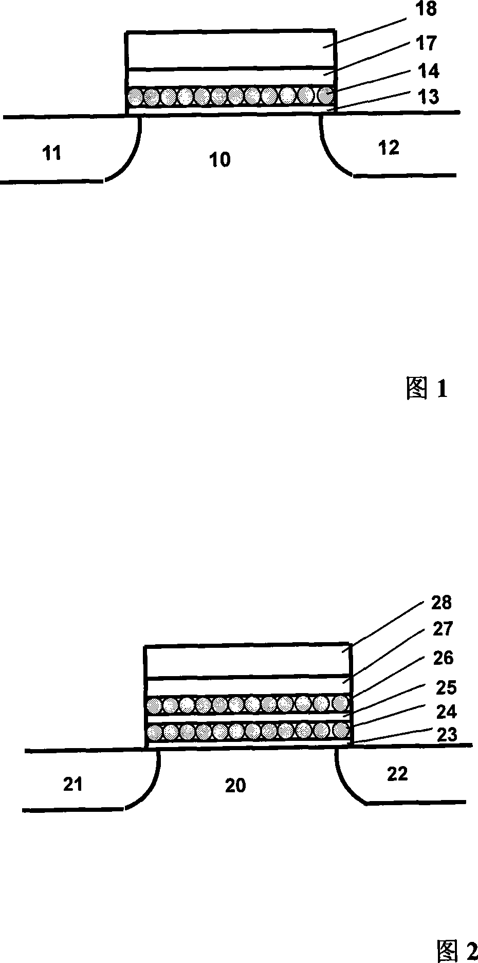
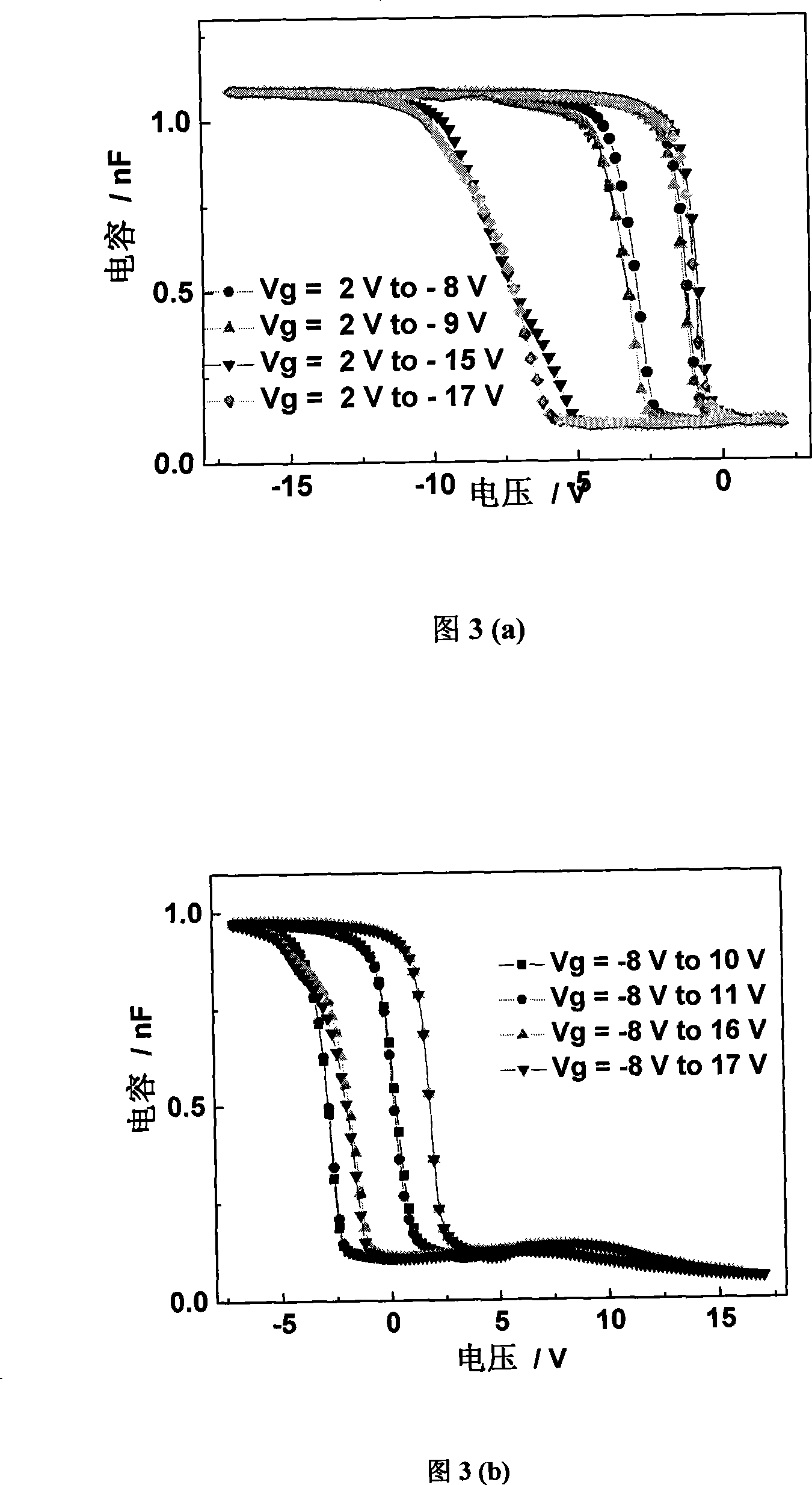
[0028] Referring to Fig. 2, the structure of the present invention: use p-type silicon (resistivity 1-10Ω·cm) as the substrate, the source and drain regions are on both sides of the substrate, and the thickness of the first layer of tunneling dielectric layer on the substrate is 1-2nm , such as 2nm SiO 2 layer; or 3-5nm, such as a 4nm SiNx layer, and then the first nano-Si layer, with a grain size of 2-7nm, such as 3 or 5nm; the second tunneling dielectric layer on the substrate is the same as the first tunneling dielectric layer; then the second nano-Si layer, with a grain size of 2-7nm, such as 3 or 5nm; deposited on the second nano-Si layer to form a silicon oxide or silicon nitride dielectric layer as a control gate, with a thickness of 10nm, 15nm also can.

[0029] 1. Use p-type silicon (resistivity 1-10Ω cm) as the substrate

[0030] 2. Formation of the first layer of tunneling dielectric layer (optional silicon oxide layer or silicon nitride layer)

[0031] 2.1 Tunne...


PUM

PropertyMeasurementUnit
electrical resistivityaaaaaaaaaa
thicknessaaaaaaaaaa
thicknessaaaaaaaaaa

Abstract

This invention relates to a semiconductor non-volatile floating grid storage based on double-layer nm Si structure, which takes p-type Si (resistivity: 1-10Ohm.cm) as a substrate and sets source and drain at either side of the substrate, and sets a SiO2 layer formed by a first tunnel dielectric layer of 1-2nm thick or a SiNx layer with the thickness of 3-5nm on the substrate, then a first Si nm layer with the grain size of 2-7nm, then a second tunnel dielectric layer of a SiO2 layer of 1-2nm thick or a SiNx layer of 3-5nm thick, then forms a second Si nm layer with the grain size of 2-7nm to be deposited to form a control SiN dielectric layer in the thickness of 8-20nm and a polysilicon grid is on the SiO or the SiN dielectric layer.

Description

technical field [0001] The invention relates to a semiconductor non-volatile floating gate memory based on nano-silicon grains, in particular to a novel semiconductor non-volatile floating-gate memory based on a double-layer nano-silicon structure and a preparation method thereof. Background technique [0002] As a typical device of non-volatile floating gate memory, flash memory (Flash memory) has been widely used in mobile electronic devices such as U disk, MP3 and mobile phones. It is promoting the modernization of people's daily life and is expected to replace personal computers in the near future. The hard disk in the computer, so that when the computer is turned on and turned off, it is not necessary to read and re-store the information in the memory from the hard disk. [0003] Research in recent years has shown that in the process of miniaturization and low power consumption of flash memory devices, they have reached the limit of nanometer...

Claims


Application Information

Patent Timeline
Patent Type & Authority Applications(China)
IPC IPC(8): H01L29/788H01L29/423H01L29/49H01L27/115H01L21/336H01L21/28H01L21/8247
Inventor 陈坤基吴良才王久敏余林蔚李伟徐骏丁宏林张贤高刘奎王祥徐岭黄信凡
Owner NANJING UNIV
Why Eureka
Try Eureka