A high speed dram architecture with uniform access latency

A dynamic random access and memory technology, applied in static memory, digital memory information, information storage, etc., can solve the problems of DRAM array bit density reduction, noise coupling mismatch, etc.

Inactive Publication Date: 2007-09-19
CONVERSANT INTPROP MANAGEMENT INC
View PDF1 Cites 75 Cited by
  • Summary
  • Abstract
  • Description
  • Claims
  • Application Information

AI Technical Summary

Problems solved by technology

However, the main disadvantage of this scheme is that compared with conventional DRAM designs, the bit density in the DRAM array is greatly reduced due to doubling the number of access transistors and bit lines per memory cell.
Moreover, such systems also use an open bitline structure, which is undesirable because the sensitivity does not match the noise coupling of the bitline pair

Method used


Image

  • A high speed dram architecture with uniform access latency
  • A high speed dram architecture with uniform access latency
  • A high speed dram architecture with uniform access latency

Examples


Embodiment Construction

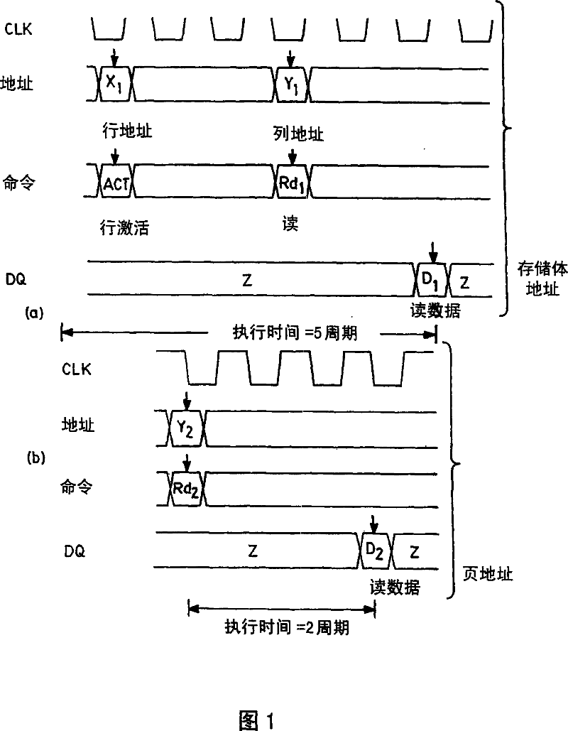
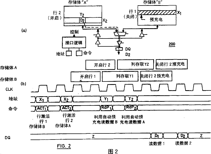
[0034] In order to obtain high-speed performance, the DRAM structure is optimized regardless of the addressing mode of its continuous memory access operations, and each read, write or refresh operation has the same timing. This is different from traditional DRAM architectures where operation timing depends on the value of the target address and the history of the last memory operation.

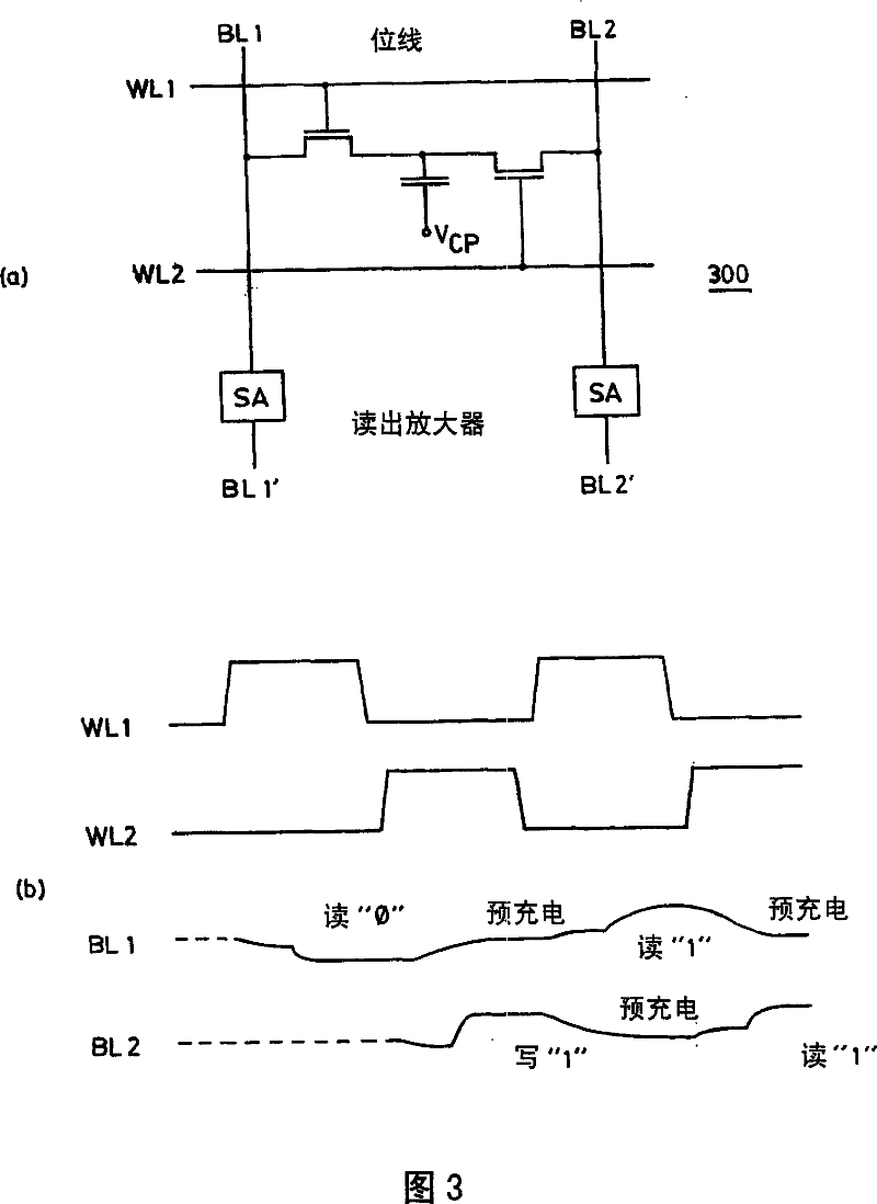
[0035] Obtaining the same access timing for all memory commands is achieved by performing a complete row access operation for each read, write or refresh command received. A complete row access operation includes word line maintenance, memory cell readout, bit line readout, cell information recovery, word line separation maintenance, and bit line compensation and pre-charging. The following description will address implementation details that allow memory devices and memory macros fabricated using conventional DRAM processing techniques to perform data accesses with execution times and cycle t...


PUM


Abstract

A Dynamic Random Access Memory (DRAM) performs read, write, and refresh operations. The DRAM includes a plurality of sub-arrays, each having a plurality of memory cells, each of which is coupled with a complementary bit line pair and a word line. The DRAM further includes a word line enable device for asserting a selected one of the word lines and a column select device for asserting a selected one of the bit line pairs. A timing circuit is provided for controlling the word line enable device, the column select device, and the read, write, and refresh operations in response to a word line timing pulse. The read, write, and refresh operation are performed in the same amount of time.

Description

[0001] This application is a divisional application of the national phase entry application 01812427.5 of the international application PCT / CA01 / 00949 filed on June 29, 2001, requiring Canadian application 2313954 filed on July 7, 2000 and Priority of US application 60 / 216679. technical field [0002] The present invention relates generally to high speed DRAM structures and, more particularly, to the timing of read, write and refresh operations. Background of the invention [0003] Traditionally, commodity designs for dynamic random access memory (DRAM) have focused less on high storage performance and more on achieving low cost-per-bit through higher overall bit density. The reason is that the cell capacity of the two-dimensional memory array increases proportionally to the square of the size, and the additional area of ​​the bit line sense amplifier, word line driver, and row address (or x address) and column address (or y address) decoder Grows proportionally to size. T...

Claims


Application Information

Patent Timeline
Patent Type & Authority Applications(China)
IPC IPC(8): G11C11/406G11C11/4076G11C11/408G11C7/22G11C8/18G11C7/10
CPCG11C8/18G11C2207/2281G11C11/406G11C7/22G11C2207/229G11C11/4076
Inventor 保罗·德蒙
Owner CONVERSANT INTPROP MANAGEMENT INC
Why Eureka
Try Eureka