Low trigger voltage silicon control rectifier and its circuit

A technology of silicon controlled rectifier and low trigger voltage, which is applied in circuits, electric solid-state devices, electrical components, etc., and can solve problems such as inability to use power protection and inability to eliminate the locked state

Inactive Publication Date: 2007-10-03
ADVANCED ANALOG TECH INC
View PDF0 Cites 15 Cited by
  • Summary
  • Abstract
  • Description
  • Claims
  • Application Information

AI Technical Summary

Problems solved by technology

That is, after ESD occurs, a surge occurs in the power supply, or a surge occurs in the circuit to be protected, the locked state cannot be elim

Method used


Image

  • Low trigger voltage silicon control rectifier and its circuit
  • Low trigger voltage silicon control rectifier and its circuit
  • Low trigger voltage silicon control rectifier and its circuit

Examples


Embodiment Construction

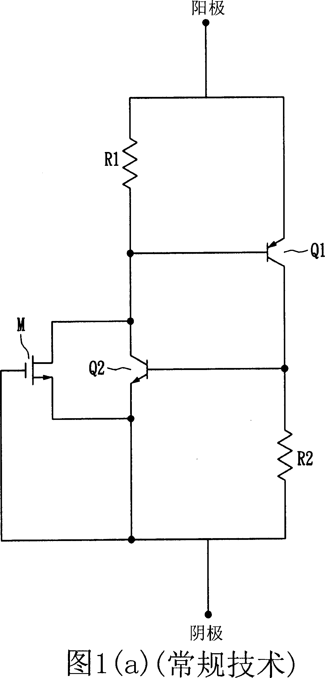
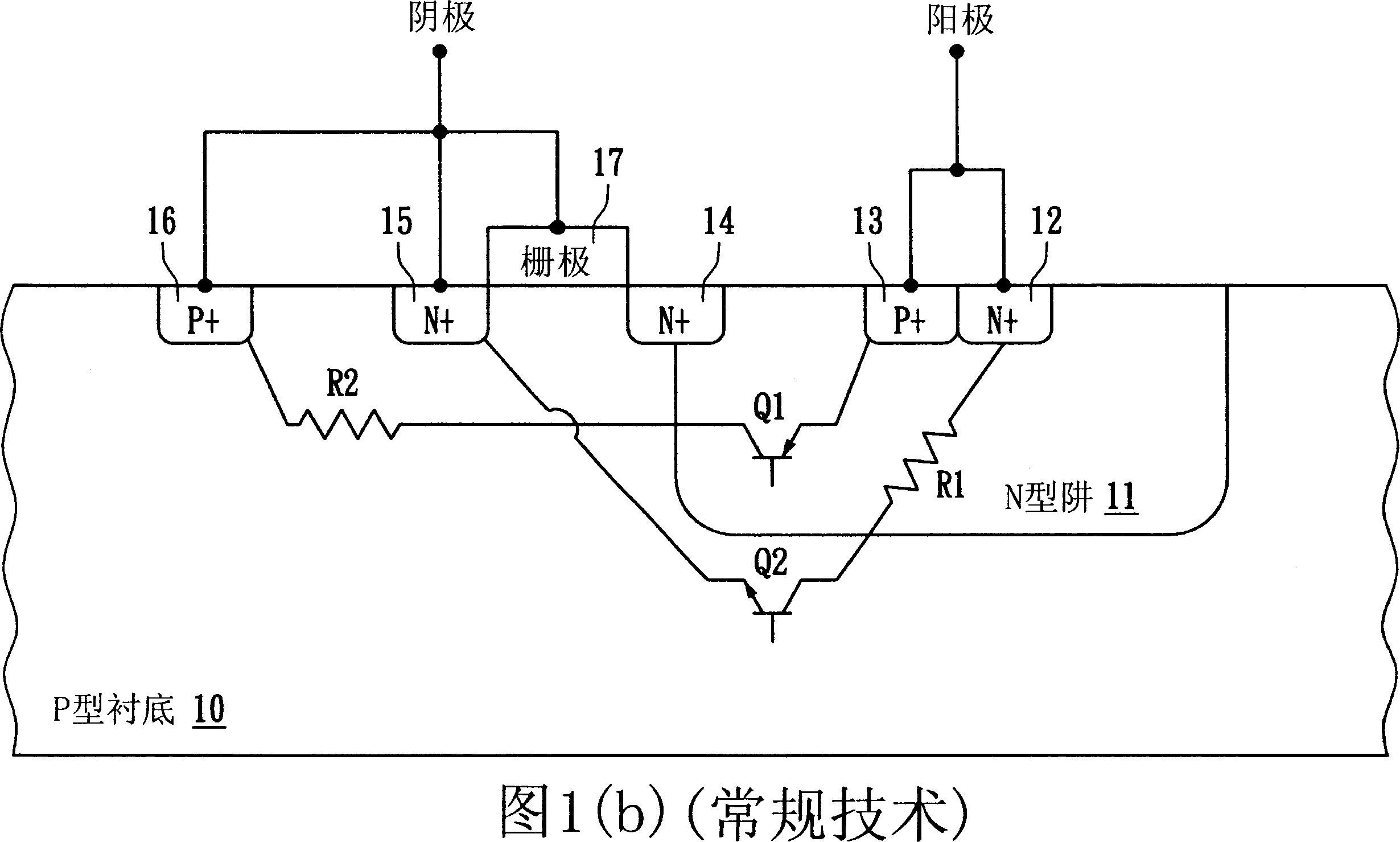
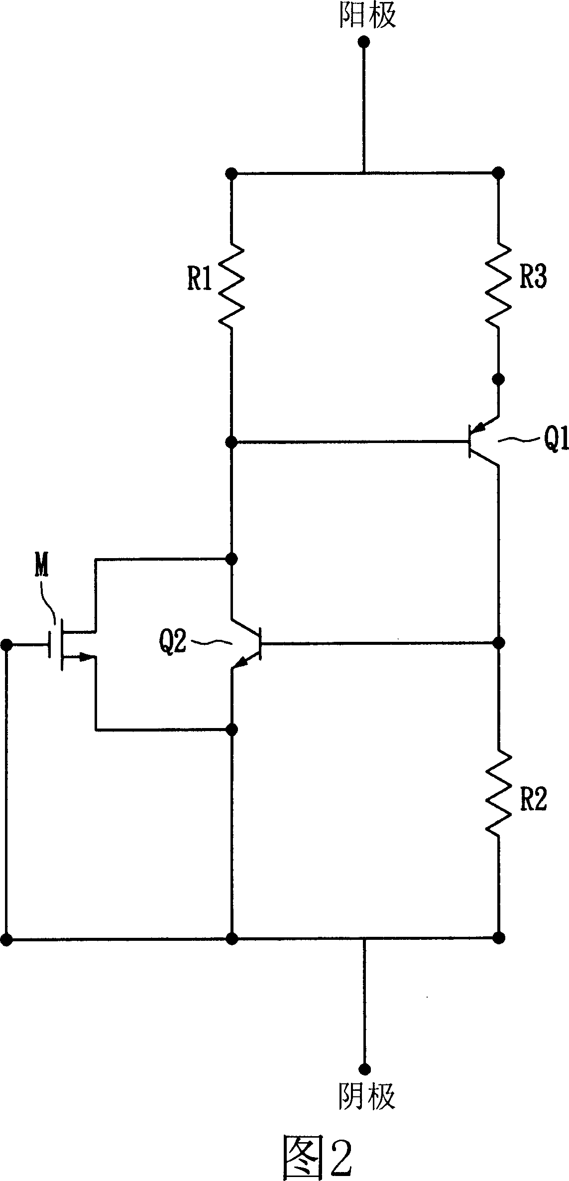
[0022] FIG. 2 is an equivalent circuit of the low trigger voltage silicon-controlled rectifier of the present invention, which adds a resistor R3 between the anode and the emitter of the parasitic bicarrier PNP transistor Q1 in the circuit of FIG. 1(a). Its operating principle is as follows. Because the breakdown voltage of the NMOS transistor M is lower than the breakdown voltage of the parasitic bicarrier NPN transistor Q2, when an ESD occurs, first the NMOS transistor M is turned on, and the current conduction acting on the NMOS transistor M will make a and The parasitic bipolar NPN transistor Q2 coupled with the resistor R2 is also turned on, and the current conduction of the parasitic bipolar NPN transistor Q2 will cause the parasitic bipolar PNP transistor Q1 to turn on. The current acting on the parasitic bipolar PNP transistor Q1 will accelerate the current conduction of the parasitic bipolar NPN transistor Q2, and finally enter into a locked state. At this time, most...


PUM


Abstract

The present invention relates to a low voltage triggering silicon controlled rectifier (SCR). It is characterized by that it utilizes addition of second doped zone which is set between the described low voltage triggering silicon controlled rectifier anode and its parasitic PNP transistor emitter to raise the holding voltage when the described low voltage triggering silicon controlled rectifier is triggered. The described low voltage triggering silicon controlled rectifier includes a semiconductor substrate with first conducting type and a grid. The described semiconductor substrate contains a first doped zone with second conducting type, a second doped zone with first conducting type, a third doped zone with second conducting type, a fourth doped zone with second conducting type and a fifth doped zone with first conducting type. The described grid is characterized by utilizing lower trigger voltage to trigger the described low voltage triggering silicon controlled rectifier.

Description

technical field [0001] The present invention relates to a low voltage triggering silicon controlled rectifier (LVTSCR), in particular to a silicon controlled rectifier with high holding voltage and low triggering voltage. Background technique [0002] In the manufacture and use of integrated circuits (ICs), the problem of Electrostatic Discharge (ESD) is often encountered. With the increasing demand for ICs with high computing speed and broadband wireless communication products, and the current IC manufacturing process is rapidly entering 80 nanometers or even below 65 nanometers, the internal components of ICs are very small, so they are easily damaged by instantaneous electrostatic discharge . Therefore, ESD has a great impact on the quality of IC, and with the continuous improvement of IC manufacturing process, the importance of ESD problem is also increasing day by day. [0003] At present, the basic specifications of the international standard for ESD protection capab...

Claims


Application Information

Patent Timeline
IPC IPC(8): H01L27/04
Inventor 杨盛渊方振宇
Owner ADVANCED ANALOG TECH INC
Why Eureka
Try Eureka