Anti-static protection structure and high-voltage integrated circuit

A high-voltage integrated circuit and protection structure technology, which is applied to circuits, electrical components, and electric solid-state devices, can solve the problem of small secondary breakdown current

Pending Publication Date: 2022-03-01
SHANGHAI HUALI MICROELECTRONICS CORP
View PDF0 Cites 0 Cited by
  • Summary
  • Abstract
  • Description
  • Claims
  • Application Information

AI Technical Summary

Problems solved by technology

[0005] However, the disadvantage of low-voltage PMOS devices is that the secondary breakdown current (It2) of the hysteresis effect is relatively small, and the trigger voltage Vt1 of low-voltage PMOS devices is mainly determined by its drain breakdown voltage (Bvdss). Therefore, when multi-stage series is used for high-voltage anti-static protection design, more series stages are required. For example, taking a 32V high-voltage process platform as an example, the trigger voltage Vt1 and maintenance voltage Vh of the low-voltage PMOS device of the high-voltage process platform About 10.5V, specifically as image 3 As shown, it is often necessary to connect 4 levels of low-voltage PMOS devices in series to achieve anti-static protection for 32V high-voltage ports.

Method used


Image

  • Anti-static protection structure and high-voltage integrated circuit
  • Anti-static protection structure and high-voltage integrated circuit
  • Anti-static protection structure and high-voltage integrated circuit

Examples


Embodiment 1

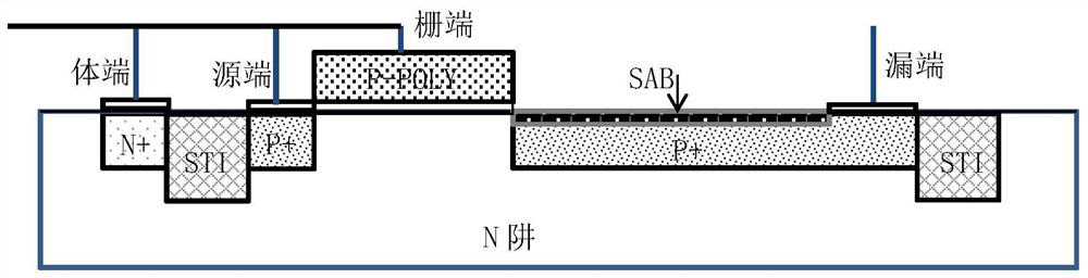
[0037] Such as Figure 4 As shown, the antistatic protection structure includes an N well 20 and a P well 30 formed in the substrate 10;

[0038] The upper and middle parts of the N well 20 and the P well 30 are separated by STI (Shallow Trench Isolation, shallow trench isolation) 40;

[0039] The lower parts of the N well 20 and the P well 30 are adjacent;

[0040] The upper part of the N well 20 is pasted with STI 40 and implanted with P-type heavy doping to form an N well P heavily doped region 24;

[0041] The upper part of the N well 20 is implanted with N-type heavy doping away from the STI 40 to form an N well N heavily doped region 22;

[0042] The upper part of the P well 30 is pasted with STI 40 and implanted with P-type heavy doping to form a P well P heavily doped region 26;

[0043] The N well P heavily doped region 24 is short-circuited with the N well N heavily doped region 22 to form an anode (anode) of the antistatic protection structure;

[0044] The P we...

Embodiment 2

[0047] Based on the antistatic protection structure of the first embodiment, the upper and middle parts of the N well 20 and the P well 30 are separated by the STI 40 .

[0048] Preferably, the N-type ion doping concentration of the N-well N heavily doped region 22 is greater than 10 times the N-type ion doping concentration of the N-well 20 .

[0049] Preferably, the P-type ion doping concentration of the N well P heavily doped region 24 and the P well P heavily doped region 26 is greater than 10 times the P type ion doping concentration of the P well 30 .

[0050] Preferably, the substrate 10 is P-type doped;

[0051] The doping concentration of the substrate 10 is smaller than that of the P-well.

Embodiment 3

[0053] Based on the antistatic protection structure of Embodiment 1, the distance a from the N well P heavily doped region 24 to the border between the N well 20 and the P well 30 is in the range of 0.2um to 2um;

[0054] The distance b from the P well P heavily doped region 26 to the border between the P well 30 and the N well 20 is in the range of 0.2um˜2um.

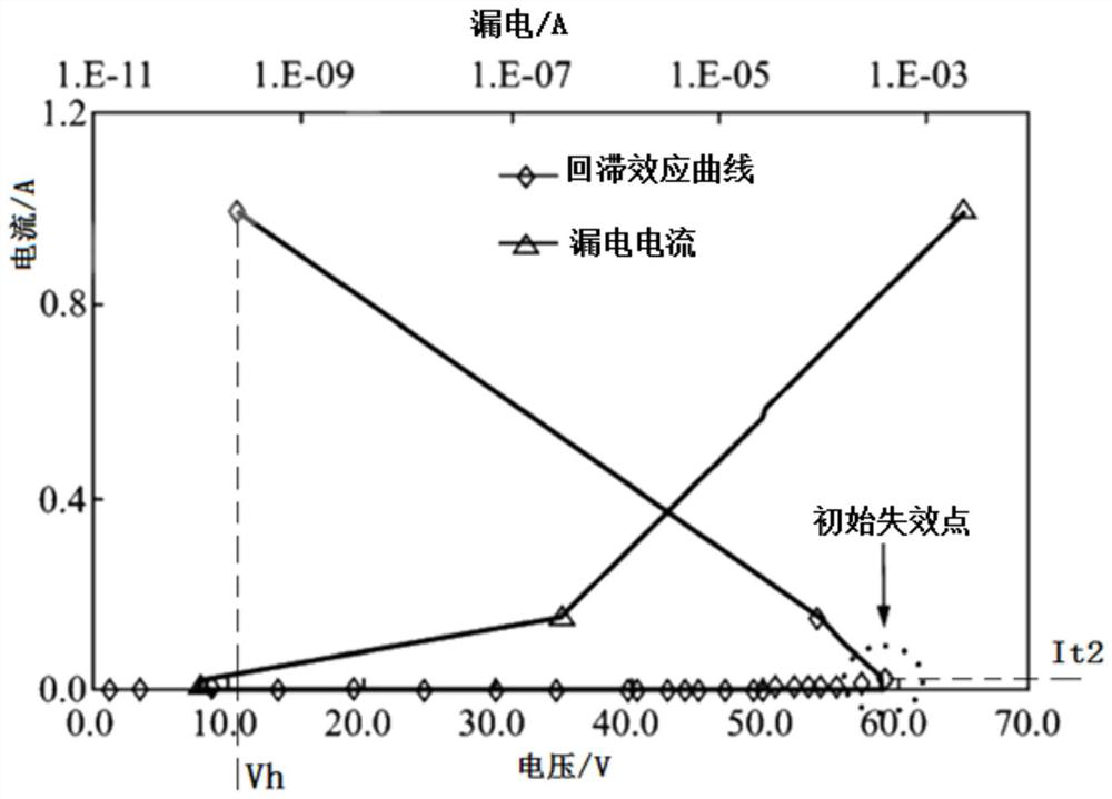
[0055] In the antistatic protection structure of the second embodiment, the trigger voltage (Vt1) is affected by parameters a and b within a certain range. Such as Figure 5 , Figure 6 As shown, in a certain process platform, when the values ​​of a and b reach 0.5um, the reverse breakdown voltage reaches 19.1V, while the trigger voltage (Vt1) and holding voltage (Vh) reach about 20V, so the anti-static The protection structure can be applied to the anti-static protection design of the 32V high-voltage port by connecting two levels in series.

[0056] Embodiment Three

[0057] The high-voltage integrated circuit ad...


PUM


Abstract

The invention discloses an anti-static protection structure. The anti-static protection structure comprises an N well and a P well which are formed in a substrate, the upper parts and the middle parts of the N well and the P well are separated by STI, and the lower parts are adjacent; sTI is attached to the upper portion of the N well, P-type heavy doping is injected, and an N well P heavy doping area is formed; n-type heavy doping is injected at the upper part of the N well far away from the STI to form an N-well N heavily doped region; sTI is attached to the upper portion of the P well, P-type heavy doping is injected, and a P well P heavy doping area is formed; the N-well P heavily doped region and the N-well N heavily doped region are short-circuited to form an anode of the anti-static protection structure; and the P heavily doped region of the P well is used as a cathode of the anti-static protection structure. According to the anti-static protection structure, no hysteresis effect can be achieved, high trigger voltage and maintaining voltage can be easily obtained, high secondary breakdown current is achieved, and when the anti-static protection structure is applied to high-voltage port anti-static protection design, the series connection number needed by multi-stage series connection and the layout area of a single-stage protection unit can be saved. The invention also discloses a high-voltage integrated circuit.

Description

technical field [0001] The invention relates to a semiconductor circuit structure, in particular to an antistatic protection structure and a high-voltage integrated circuit. Background technique [0002] The anti-static protection design of high-voltage circuits has always been a technical problem, because the core of high-voltage circuits: high-voltage devices (for example, LDMOS (Laterally Diffused Metal Oxide Semiconductor)) are not suitable for ordinary low-voltage devices. For anti-static protection design, because the characteristics shown by the hysteresis effect curve of high-voltage devices are very poor. Depend on figure 1 The hysteresis effect curve of the conventional high-voltage device LDMOS can be drawn as follows: 1) The holding voltage (Vh) is too low, often much lower than the operating voltage of the high-voltage circuit, and it is easy to cause the latch-up effect when the high-voltage circuit works normally; 2) The secondary The breakdown current (ther...

Claims


Application Information

Patent Timeline
Patent Type & Authority Applications(China)
IPC IPC(8): H01L27/02
CPCH01L27/0296H01L27/0274H01L29/861H01L29/0649H01L27/0292
Inventor 朱天志
Owner SHANGHAI HUALI MICROELECTRONICS CORP
Why Eureka
Try Eureka