Polysilicon dummy gate electrostatic discharge device with increased sustain voltage and manufacturing method thereof

A technology of maintaining voltage and electrostatic discharge, which is applied in the fields of electric solid-state devices, semiconductor/solid-state device manufacturing, electrical components, etc. Effects of ESD Robustness

Active Publication Date: 2020-10-30
HUNAN NORMAL UNIVERSITY
View PDF4 Cites 0 Cited by
  • Summary
  • Abstract
  • Description
  • Claims
  • Application Information

AI Technical Summary

Problems solved by technology

However, LDMOS-SCR still has the problem of uneven conduction of the interdigitated fingers of the device, that is, the ESD discharge capability of the device does not increase linearly with the number of interdigitated fingers of the device, and the direct way to solve the uneven conduction of the LDMOS-SCR is to improve this The maintenance voltage of the device, so that the value of the maintenance voltage of the turned-on fork fingers will reach the value of the trigger voltage again, so that the rest of the unopened fork fingers are turned on

Method used


Image

  • Polysilicon dummy gate electrostatic discharge device with increased sustain voltage and manufacturing method thereof
  • Polysilicon dummy gate electrostatic discharge device with increased sustain voltage and manufacturing method thereof
  • Polysilicon dummy gate electrostatic discharge device with increased sustain voltage and manufacturing method thereof

Examples


Embodiment Construction

[0032] The present invention will be further described below in conjunction with the accompanying drawings and embodiments.

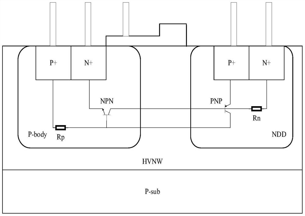
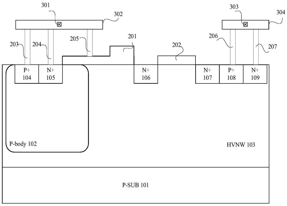
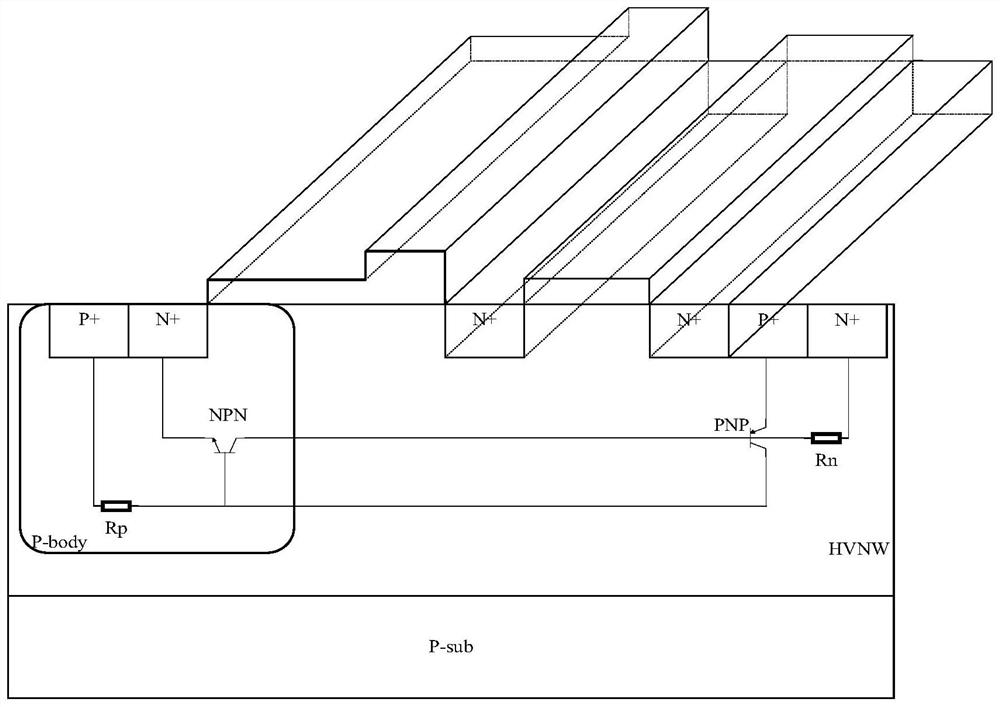
[0033] Such as figure 2 , image 3 As shown, a polysilicon dummy gate ESD device with increased sustain voltage includes substrate P-SUB101, P-body region 102, HVNW region 103, first P+ implantation region 104, first N+ implantation region 105, second N+ implanted region 106, third N+ implanted region 107, second P+ implanted region 108, fourth N+ implanted region 109, first polysilicon gate 201, second polysilicon dummy gate 202, the substrate P-SUB 101 A HVNW region 103 is arranged in the middle, and a P-body region 102 is arranged in the left half of the HVNW region 103. In the P-body region 102, a first P+ implantation region 104, a first N+ implantation region 105, and a A polysilicon gate 201 spans the junction of the P-body region 102 and the HVNW region 103, and the second N+ implantation region 106 and the second polysilicon dummy gate 202 a...


PUM


Abstract

The invention discloses a polysilicon pseudo-gate electrostatic discharge device for improving a maintaining voltage. The electrostatic discharge device comprises a substrate; an HVNW region is arranged in the substrate; a P-body region is arranged in the left half part of the HVNW region; a first P+ injection region and a first N+ injection region are arranged in the P-body region; a first polysilicon gate stretches across the junction of the P-body region and the HVNW region; a second N+ injection region, a second polysilicon pseudo gate, a third N+ injection region, a second P+ injection region and a fourth N+ injection region are arranged in the right half part of the HVNW region; and the second polysilicon pseudo gate forms the polysilicon pseudo-gate structure. The device disclosed in the invention adopts the polysilicon pseudo-gate structure, so that ESD of the LDMOS-SCR device structure can be far from the surface of a channel, and the majority of ESD current stress can be released from the device structure, so that the device structure can bear high enough electrostatic discharge pulse stress, thereby preventing thermal breakdown from occurring on the surface of the device.

Description

technical field [0001] The invention relates to the field of integrated circuits, in particular to a polysilicon pseudo-gate electrostatic discharge device with increased sustain voltage and a manufacturing method thereof. Background technique [0002] In the past few years, integrated circuits have been used in people's normal lives, greatly improving people's quality of life and efficiency. The development of integrated circuits still follows the direction guided by Moore's Law, that is, devices are smaller in size and more integrated. high. Electrostatic discharge (ESD) is one of the main reasons for the failure of integrated circuits, and with the progress of semiconductor technology, ESD protection has been paid more and more attention. According to relevant statistics, in the field of microelectronics, the proportion of electronic products that fail due to ESD problems is about With 58%, this data fully demonstrates the importance of ESD protection in integrated circu...

Claims


Application Information

Patent Timeline
Patent Type & Authority Patents(China)
IPC IPC(8): H01L27/02H01L21/8249
CPCH01L21/8249H01L27/0262H01L27/0266H01L27/0296
Inventor 金湘亮汪洋
Owner HUNAN NORMAL UNIVERSITY
Why Eureka
Try Eureka