Current controlled full-balance differential current transmitter

A current transmitter and current control technology, applied in the direction of logic circuits using specific components, logic circuits using semiconductor devices, etc., can solve problems such as adjustment, inability to provide the ability to suppress interference signals, and control port characteristics.

Inactive Publication Date: 2007-10-03
HUNAN UNIV
View PDF0 Cites 13 Cited by
  • Summary
  • Abstract
  • Description
  • Claims
  • Application Information

AI Technical Summary

Problems solved by technology

However, in analog-digital hybrid circuits, since non-ideal signals are easily generated, and digital circuit blocks generate noise due to clock signal feeding and charge injection
This noise not only affects the digital circuit module, but also affects the analog circuit part and the radio frequency circuit part through substrate crosstalk, circuit coupling, etc., and the second-generation current transmitter cannot provide a good ability to suppress interference signals. In addition, it cannot pass through The external current is used to control its port characteristics, that is, the parameters of the CCII cannot be adjusted by the external bias current or voltage, so that the application of the second-generation current transmitter and the filter circuit formed by it is greatly restricted.

Method used


Image

  • Current controlled full-balance differential current transmitter
  • Current controlled full-balance differential current transmitter
  • Current controlled full-balance differential current transmitter

Examples


Embodiment Construction

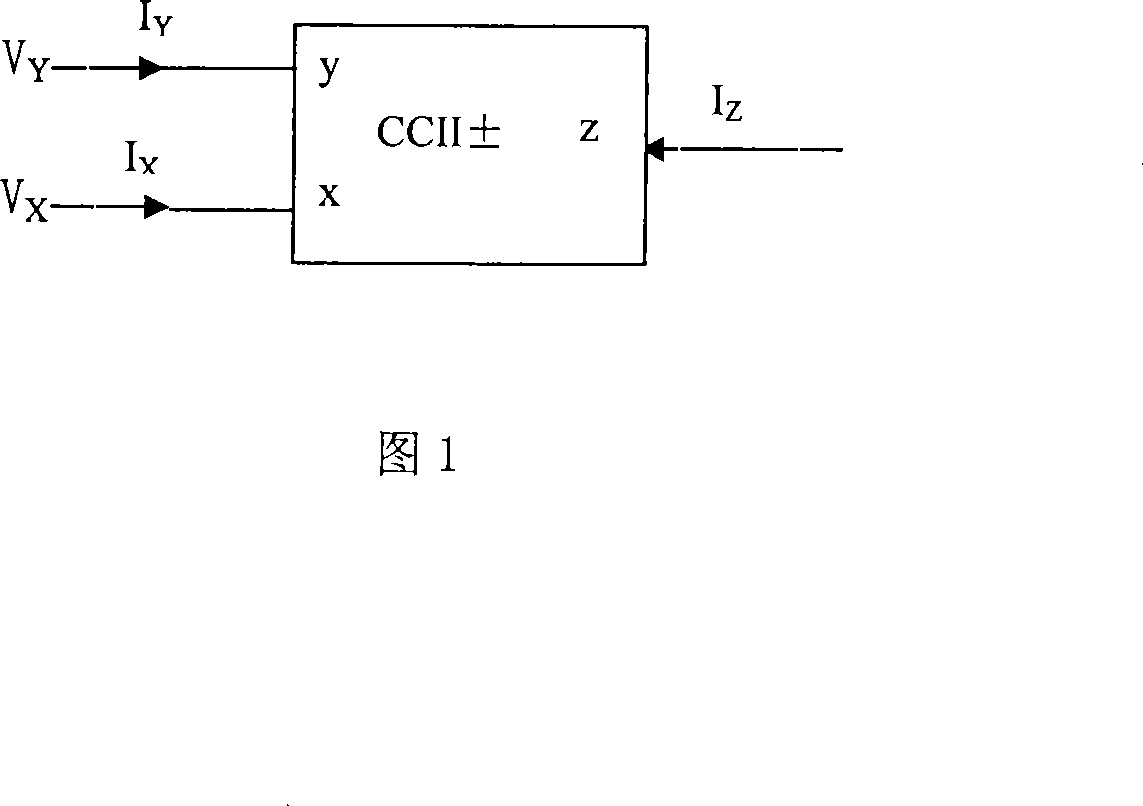
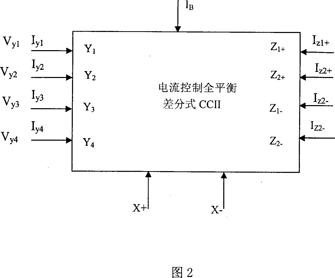
[0019] Figure 2 is the circuit symbol of a current-controlled fully balanced current transmitter, including two pairs of high-impedance differential voltage input terminals Y 1 ~Y 4 , two voltage tracking terminals X + 、X - , a pair of non-inverting current output terminals Z 1+ ,Z 2+ , a pair of inverting current output terminals Z 1- ,Z 2- , and a current control terminal. due to relationship R x = V T 2 I B The existence of the current control terminal can control the parasitic resistance R of the current input terminal x , and then control the voltage-current relationship between the X terminal and the Y terminal. Its transmission characteristics are shown in formulas (1) and (2).

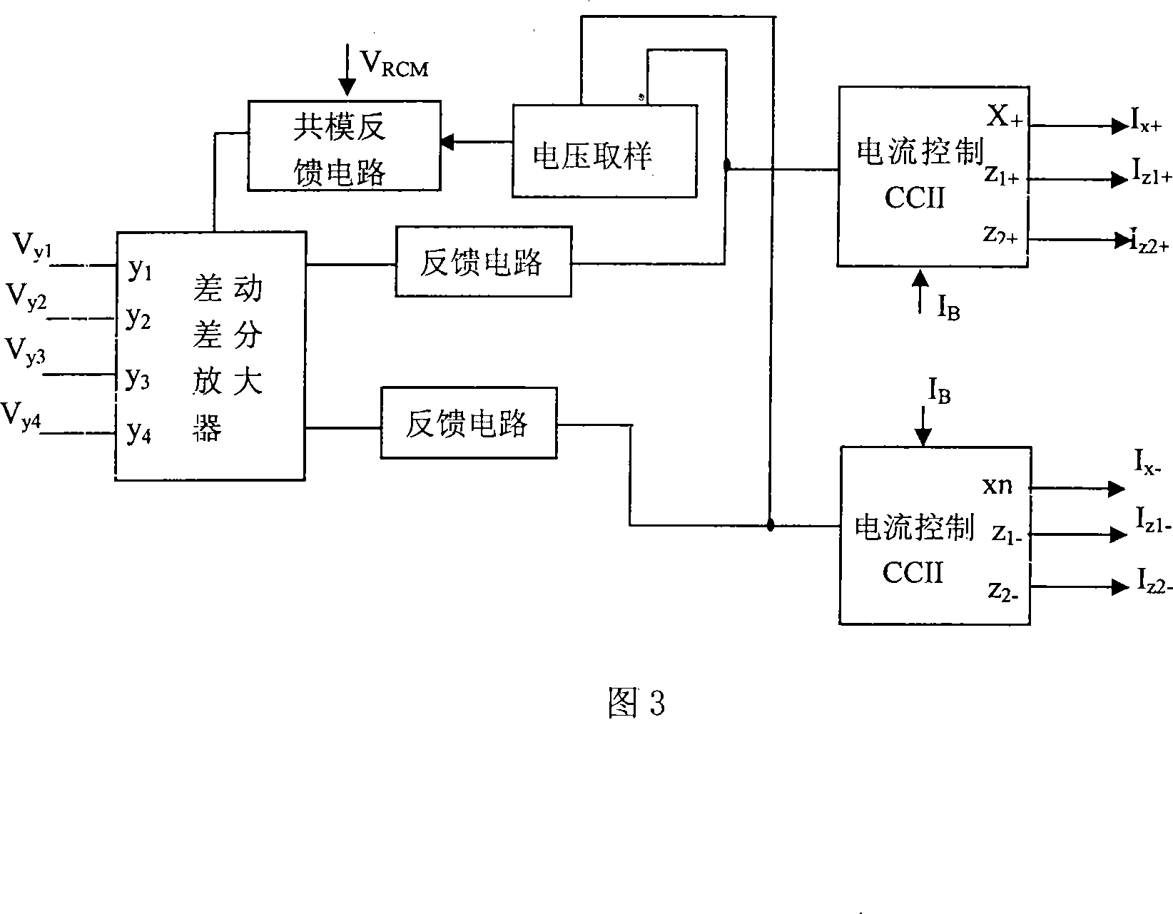
[0020] Fig. 3 is a schematic diagram of the main structure of the present invention, the circuit mainly ...


PUM


Abstract

A current transmission unit of current control in all-balance differential mode consists of a pair of voltage differential input ends, high input impedance, a pair of differential voltage tracking ends, a pair of current output ends with the same phase and a pair of current output ends with opposite phase. It is featured as enabling to control relation of voltage at a pair of differential voltage tracking ends to differential voltage at a pair of voltage differential input ends by regulating bias current of the circuit.

Description

technical field [0001] The technology relates to a differential current transmitter, in particular to a second-generation CMOS current transmitter with electronic control and capable of effectively suppressing common-mode signals, and belongs to the field of analog integrated circuits. Background technique [0002] The second generation current conveyor (CCII) is a circuit block proposed by A.S.Sedra and K.C.Smith in 1970. Figure 1 is the circuit symbol of the second-generation current conveyor. As shown in Figure 1, the second-generation current conveyor has a current input terminal X, a voltage input terminal Y, and a positive current output terminal Z + , an inverting current output Z - . The transfer characteristics of this second generation current conveyor are as follows: [0003] (1) The Y input terminal is a high-impedance input terminal, and its input current is zero, and I Y = 0; [0004] (2) Apply a voltage V to the Y input terminal Y , then the voltage at t...

Claims


Application Information

Patent Timeline
Patent Type & Authority Applications(China)
IPC IPC(8): H03K19/08
Inventor 王春华李仁发何松华张秋晶何海珍李涛易波何选森
Owner HUNAN UNIV
Why Eureka
Try Eureka