
Pixel array substrate

A pixel array substrate and substrate technology, which is applied in the directions of optics, instruments, electrical components, etc., can solve the problems of large display gaps in the pixel area and disconnection of data lines, etc.

Active Publication Date: 2007-10-10
AU OPTRONICS CORP
View PDF0 Cites 21 Cited by
  • Summary
  • Abstract
  • Description
  • Claims
  • Application Information

AI Technical Summary

Problems solved by technology

[0015] In view of this, the main purpose of the present invention is to provide a pixel array substrate, which can solve the problem of disconnection of data lines
[0016] Another object of the present invention is to provide a pixel array substrate, which can solve the problem of excessive display gap in the damaged pixel area

Method used


Image

  • Pixel array substrate
  • Pixel array substrate
  • Pixel array substrate

Examples


no. 1 example

[0073] 3A is a partial top view of the pixel array substrate according to the first embodiment of the present invention, and FIG. 3B is a cross-sectional view of the pixel array substrate in FIG. 3A, wherein the section line is the line BB' in FIG. 3A. Please refer to FIG. 3A and FIG. 3B, the pixel array substrate 300a of the present invention includes a substrate 310 and a plurality of scanning lines 320, a plurality of data lines 330, a plurality of active elements 340, a plurality of pixel electrodes 350, A plurality of first patterned floating metals 360 and a plurality of first patterned connecting wires 370 . Wherein, a first insulating layer 391 is formed between the first patterned floating metal 360 and the data line 330, a second insulating layer 392 is formed above the data line 330, and a semiconductor layer is formed above the scanning line 220 of the active element 340. 393 on the first insulating layer 391. These data lines 330 and scan lines 320 form a plurali...

no. 2 example

[0080] FIG. 4 is a partial top view of a pixel array substrate according to a second embodiment of the present invention. Referring to FIG. 4 , the pixel array substrate 300b of this embodiment is similar to the pixel array substrate 300a of the first embodiment (as shown in FIG. 3A ). In this embodiment, a part of the pixel electrode 350 overlaps with the scan line 320 and forms an auxiliary capacitor 351 . Wherein, the pixel array substrate 300a further includes a plurality of contact windows 372 disposed on the substrate 310, and the contact windows 372 are electrically connected to the partially overlapping first patterned floating metal 360 and the first patterned connection wire 370. between. In other words, the first patterned floating metal 360 and the first patterned connection wire 370 on the same row have already passed through the contact window 372 to form wires similar to the parallel data lines 330 during fabrication.

[0081] Following the above, when the dis...

no. 3 example

[0084] 5A is a partial top view of a pixel array substrate according to a third embodiment of the present invention. Please refer to FIG. 5A , the pixel array substrate 300c of this embodiment is similar to the pixel array substrate 300a of the first embodiment (as shown in FIG. 3A ), the difference is that the first patterned floating metal 360 of this embodiment has a second A protrusion 366. In addition, the active element 340 is, for example, a thin film transistor, wherein the gate 342 of the active element 340 is electrically connected to the scan line 320 (in this embodiment, the gate 342 of the active element 340 is, for example, formed by a part of the scan line 320 formed), and the source 344 of the active element 340 is electrically connected to the data line 330 , and the drain 346 of the active element 340 is electrically connected to the pixel electrode 350 . In addition, the first protrusion 366 partially overlaps the drain 346 of the active device 340 .

[00...


PUM


Abstract

The pixel array base plate includes base plate and following parts configured on the base plate: scanning wires, data wires, active elements, pixel electrodes, multiple first patternized floating placed metals, and multiple first patternized connection conducting wires. Being in crisscross mode, data wires and scanning wires form multiple pixel areas. Each active element connects corresponding scanning wire, data wire and pixel electrode electrically. Moreover, each first patternized floating placed metal and any data wire are overlapped partially. Crossing over any one scanning wire, each first patternized connection conducting wire and first patternized floating placed metal on two sides of scanning wire are overlapped partially.

Description

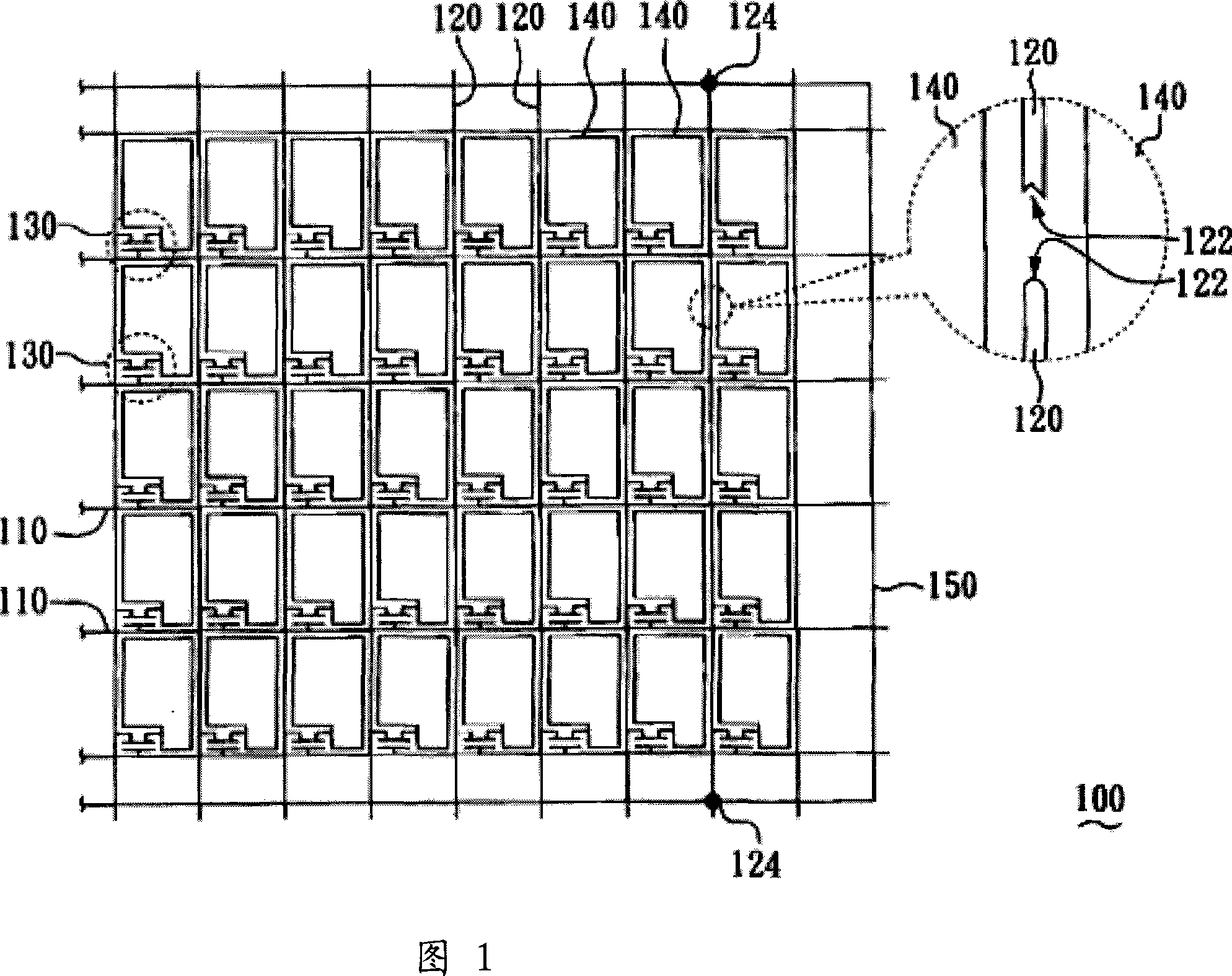
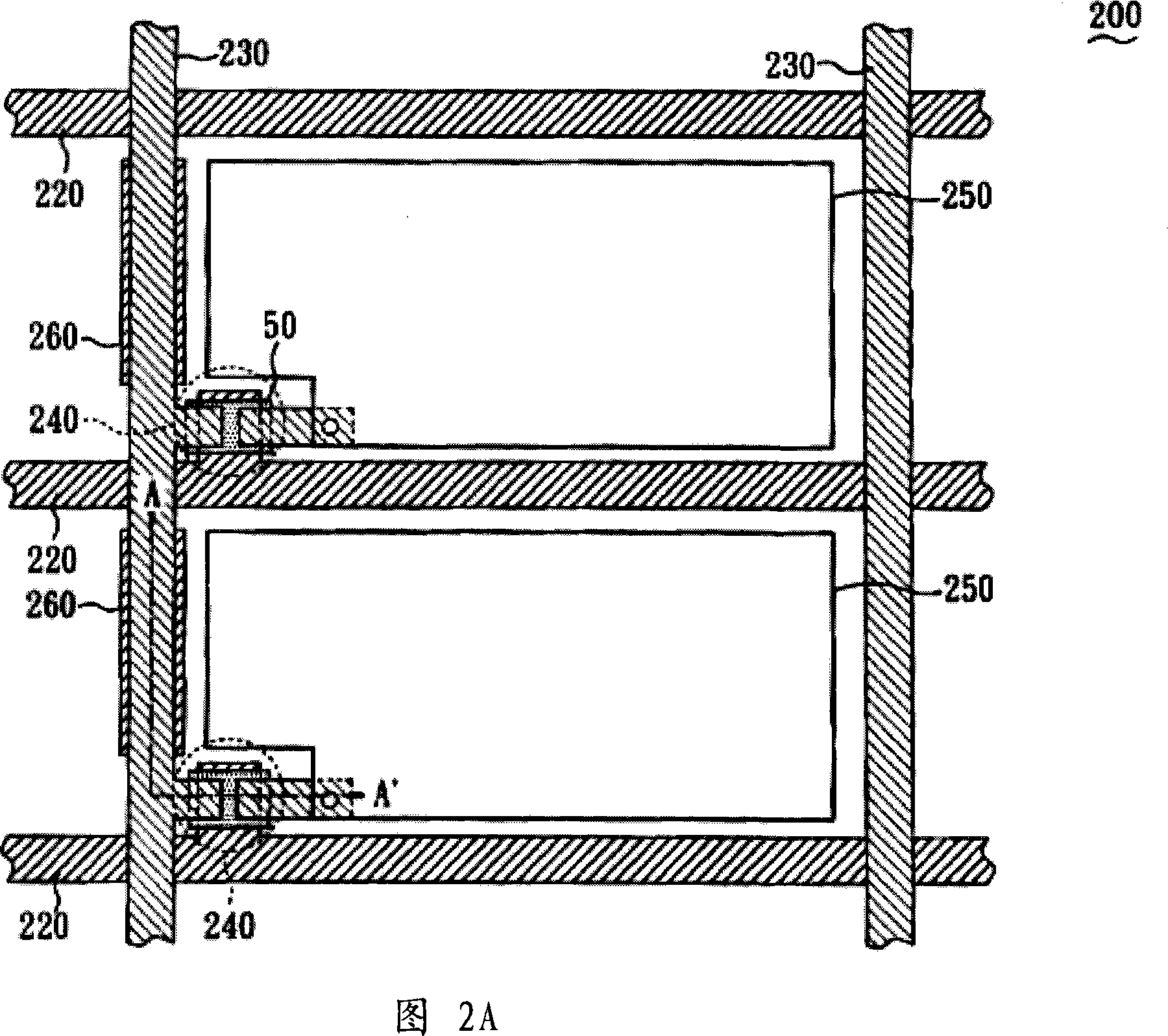
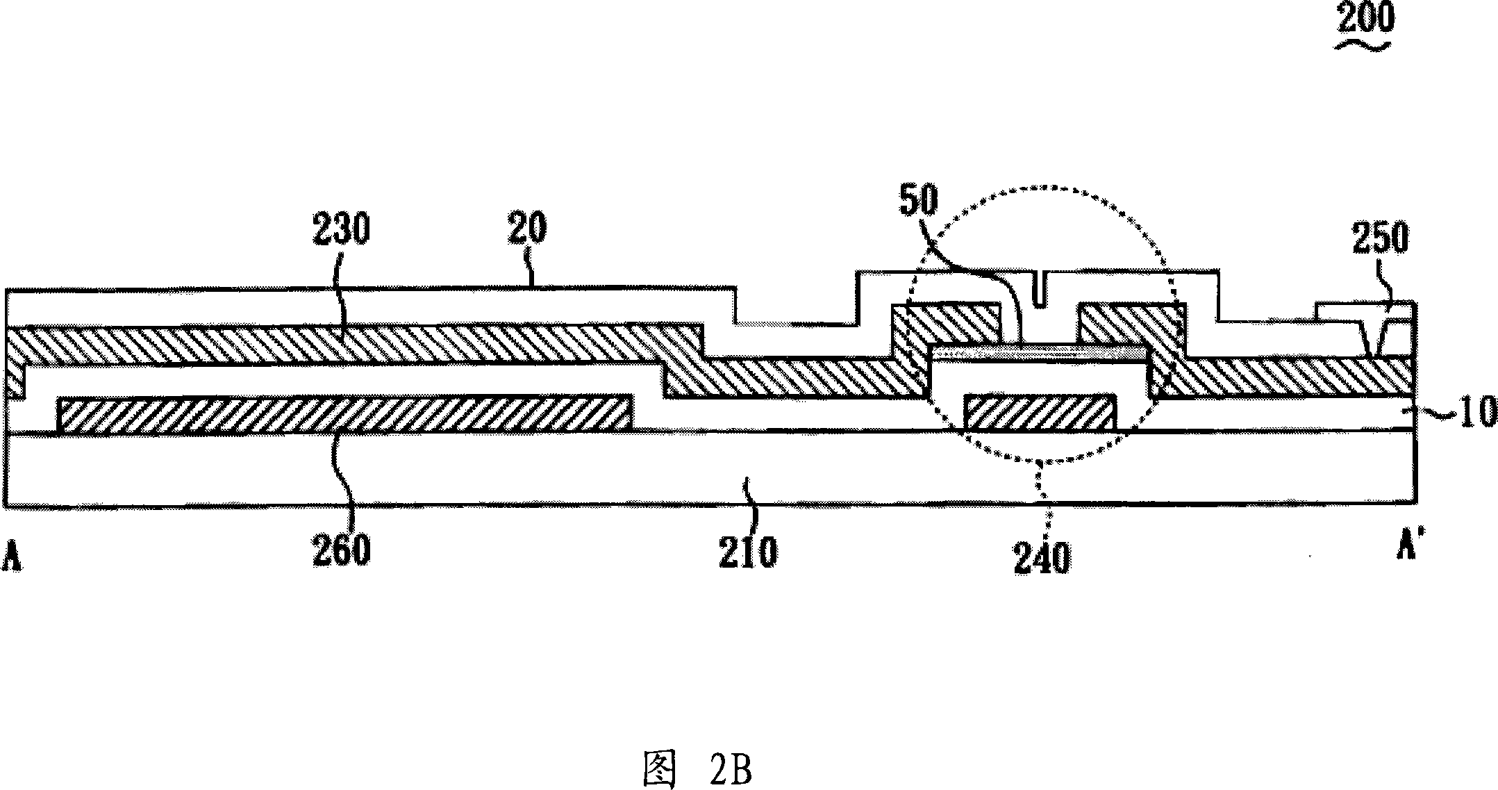
technical field [0001] The invention relates to a semiconductor element substrate, and in particular to a pixel array substrate. Background technique [0002] With the advancement of modern video technology, various displays have been widely used on the display screens of consumer electronic products such as mobile phones, notebook computers, digital cameras and personal digital assistants (PDAs). Among these displays, liquid crystal displays (LCDs) and organic electroluminescent displays (OLEDs) have become the mainstream in the market due to their advantages of light weight, small volume, and low power consumption. Whether it is a liquid crystal display or an organic electroluminescent display, the manufacturing process includes forming a pixel array substrate by semiconductor technology. By correspondingly adjusting the colors displayed by each pixel in the pixel array substrate, the display can generate images. [0003] FIG. 1 is a partial top view of a known pixel arr...

Claims


Application Information

Patent Timeline
IPC IPC(8): H01L27/12H01L23/528G02F1/1362
Inventor 陈建州邱俊昌
Owner AU OPTRONICS CORP
Learn More