Amorphous zinc oxide thin film transistor and method of manufacturing the same

A thin-film transistor and amorphous technology, which is applied in the field of low-temperature ZnO TFT and its manufacturing, can solve the problems of being unsuitable for mass production and unfavorable for large-screen displays.

Inactive Publication Date: 2007-10-24
SAMSUNG ELECTRONICS CO LTD
View PDF1 Cites 36 Cited by
  • Summary
  • Abstract
  • Description
  • Claims
  • Application Information

AI Technical Summary

Problems solved by technology

This method is disadvantageous for manufacturing large screen displays
In particular, t

Method used


Image

  • Amorphous zinc oxide thin film transistor and method of manufacturing the same
  • Amorphous zinc oxide thin film transistor and method of manufacturing the same
  • Amorphous zinc oxide thin film transistor and method of manufacturing the same

Examples


Embodiment Construction

[0019] To briefly describe the present invention, a semiconductor channel is formed using a low temperature process at or below 350°C, and the semiconductor channel has n(GaO 3 )·m(InO 3 )·(ZnO)k composition, wherein the inequality conditions n≥1.5, m≥1.5, k>0 are satisfied. Here, k in the inequality has a different value from at least one of m and n.

[0020] According to an embodiment of the present invention, using a sputtering process which is a low-temperature process, specifically a radio frequency (RF) magnetron sputtering method, a ZnO TFT is formed, which has a GaO 3 -InO 3 -Amorphous semiconductor channel formed of ZnO semiconductor material.

[0021] Hereinafter, the present invention will be described more fully with reference to the accompanying drawings, in which exemplary embodiments of the invention are shown.

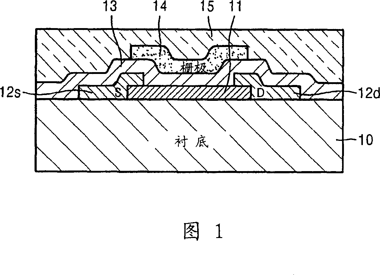
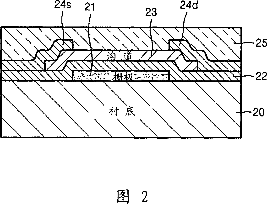
[0022] 1 is a schematic cross-sectional view of a top-gate ZnO TFT according to an embodiment of the present invention, and FIG. 2 is a schematic c...


PUM


Abstract

The invention provides an amorphous zinc oxide (ZnO) thin-film transistor (TFT) and a manufacturing method thereof. The amorphous zinc oxide thin-film transistor comprises an underlay, a semiconductor channel, a source electrode, a drain electrode, a grid electrode and a grid electrode insulator, wherein, the underlay is formed by amorphous zinc oxide compound semiconducting material containing n (Gao3), m (InO3) and (ZnO) k; the source electrode and the drain electrode are electrically contacted with the two ends of the semiconductor channel; the grid electrode forms an electric field surrounding the semiconductor channel; the grid electrode insulator is arranged between the grid electrode and the semiconductor channel. The conditions of inequality that n is more than or equal to 1.5, m is more than or equal to 1.5 and k is more than zero are met.

Description

technical field [0001] The present invention relates to a zinc oxide (ZnO) thin film transistor (TFT), and more particularly, to a low-temperature ZnO TFT and a manufacturing method thereof. Background technique [0002] Amorphous silicon TFTs can be fabricated using a low temperature process, but such TFTs have very low mobility and do not satisfy constant current bias conditions. Polysilicon TFTs have high mobility and satisfy a constant current test condition, but do not have uniform characteristics. Thus, the polysilicon TFT cannot have a large area and requires a high temperature process. ZnO, which is used as a metal oxide semiconductor material instead of a silicon semiconductor material, is applied to TFTs, sensors, optical waveguides, piezoelectric elements, and the like. [0003] Materials forming a general ZnO TFT will now be described. The channel is formed of ZnO, and a source and a drain contacting both ends of the channel and a gate forming an electric fiel...

Claims


Application Information

Patent Timeline
IPC IPC(8): H01L29/786H01L21/336
Inventor 金昌桢宋利宪姜东勋朴永洙
Owner SAMSUNG ELECTRONICS CO LTD
Why Eureka
Try Eureka