Inductor element and method for production thereof, and semiconductor module with inductor element

A technology of inductance components and semiconductors, applied in the fields of semiconductor devices, semiconductor/solid-state device manufacturing, semiconductor/solid-state device components, etc., can solve the problem of insufficient sintering of the ferrite magnetic layer, etc. The effect of the high quality factor

Inactive Publication Date: 2007-10-31
SONY CORP
View PDF7 Cites 15 Cited by
  • Summary
  • Abstract
  • Description
  • Claims
  • Application Information

AI Technical Summary

Problems solved by technology

However, these metals are sintered at relatively low temperatures, which are insufficient to completely sinter the ferrite magnetic layer 72

Method used


Image

  • Inductor element and method for production thereof, and semiconductor module with inductor element
  • Inductor element and method for production thereof, and semiconductor module with inductor element
  • Inductor element and method for production thereof, and semiconductor module with inductor element

Examples


Embodiment Construction

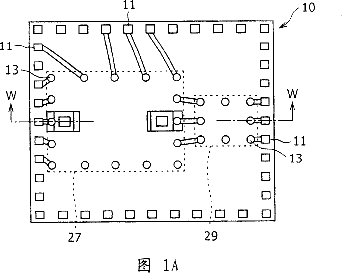
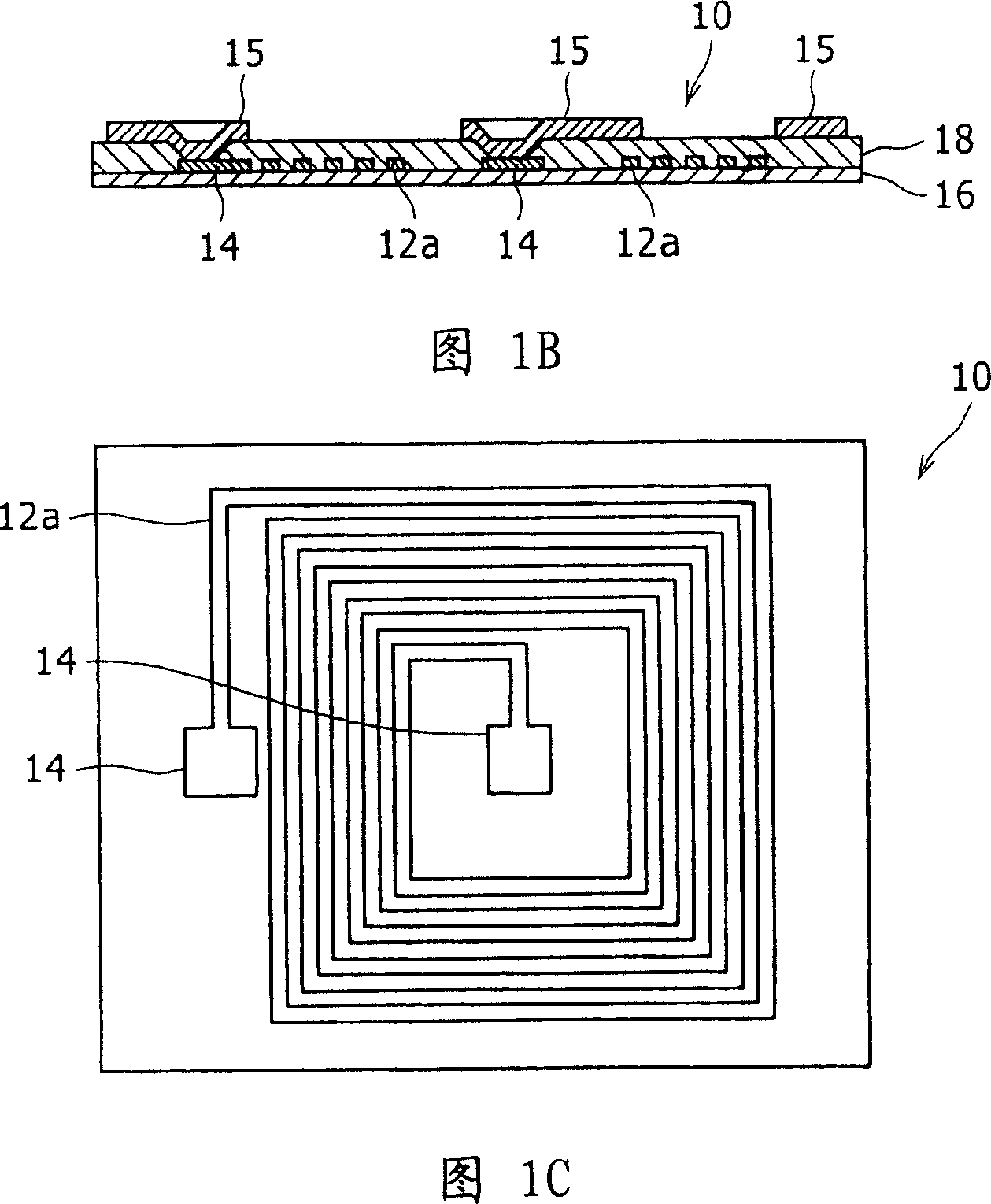
[0061] An inductance element according to an embodiment of the present invention should have both a magnetic material substrate and a magnetic material layer formed of a high magnetic permeability material such that the coil is embedded within the high magnetic permeability material. This structure makes the inductance element exhibit a large inductance.

[0062] Both the magnetic material substrate and the magnetic material layer should preferably be formed of ferrite. The magnetic material having a thickness of 50 μm formed of ferrite by aerosol deposition has a compact structure, so that the inductance element is thin and small in size but has a large inductance.

[0063] The coil should preferably be a planar coil thicker than 50 μm so that it has a large cross-sectional area to allow a large allowable current (maximum current) to flow through the inductive element.

[0064] The inductive element should have a terminal connected to the end of the coil on the outside of th...


PUM

PropertyMeasurementUnit
thicknessaaaaaaaaaa
thicknessaaaaaaaaaa
diameteraaaaaaaaaa

Abstract

An inductor element includes a substrate of magnetic material, a coil, and a layer of magnetic material. The coil of conductive material is formed on the substrate. The layer of magnetic material is so formed by aerosol deposition as to enclose the coil on the substrate of magnetic material.

Description

technical field [0001] The present invention relates to electronic components, in particular to a small-sized inductor element with large inductance and high quality factor and its manufacturing method, and to a semiconductor module with the inductor element. Background technique [0002] Inductors are classified into several types according to their structure, such as wire wound coils, laminated coils, and thin film coils. The laminated coil is composed of multiple layers of ferrite or ceramic materials stacked on each other, and conductor patterns are printed on each layer, so that all printed conductor patterns are connected to each other through via contacts. A thin film coil is a helical planar coil held between layers of ferrite or ceramic material. Thin film coils are further classified into two categories, such as closed magnetic circuit and open magnetic circuit, according to whether the coil is isolated from the surrounding environment. In a closed magnetic circu...

Claims


Application Information

Patent Timeline
Patent Type & Authority Applications(China)
IPC IPC(8): H01F17/00H01F1/10H01F5/04H01F1/113H01F41/00
CPCH01L2924/19107H01L24/48H01L2924/3025H01L2924/15311H01L2924/19106H01F2017/0066H01L2224/16H01L2924/09701H01L2224/45147H01L21/563H01F1/344H01L2924/01046H01L23/3128H01L2924/01079H01L2224/48091H01L25/0655H01L23/14H01L2924/19041H01F17/0006H01F41/046H01L2924/01078H01L23/645H01L2224/73203H01L2224/16225H01L2924/19105H01L2924/30107H01L2924/01015H01L2924/01047H01L2924/00014H01L24/45H01L2924/181H01L2224/32225H01L2224/73204H01L2924/00011Y10T29/4902H01L2924/15192H01L2224/16265H01L2924/00H01L2224/45099H01L2924/00012H01L2924/01005H01L27/02H01F17/00
Inventor 大矢洋一柳川周作冈修一
Owner SONY CORP
Why Eureka
Try Eureka