Method of fabricating recess channel in semiconductor device

A technology for semiconductors and devices, applied in the field of manufacturing semiconductor devices, can solve the problems of reducing reproducibility, defects in product characteristics, etc.

Inactive Publication Date: 2007-10-31
SK HYNIX INC
View PDF1 Cites 8 Cited by
  • Summary
  • Abstract
  • Description
  • Claims
  • Application Information

AI Technical Summary

Problems solved by technology

Therefore, the characteristics of the resulting product will be defective and will reduce the reproducibility

Method used


Image

  • Method of fabricating recess channel in semiconductor device
  • Method of fabricating recess channel in semiconductor device
  • Method of fabricating recess channel in semiconductor device

Examples


Embodiment Construction

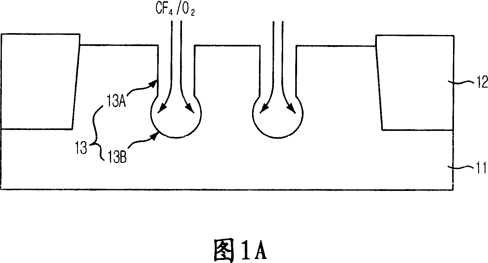
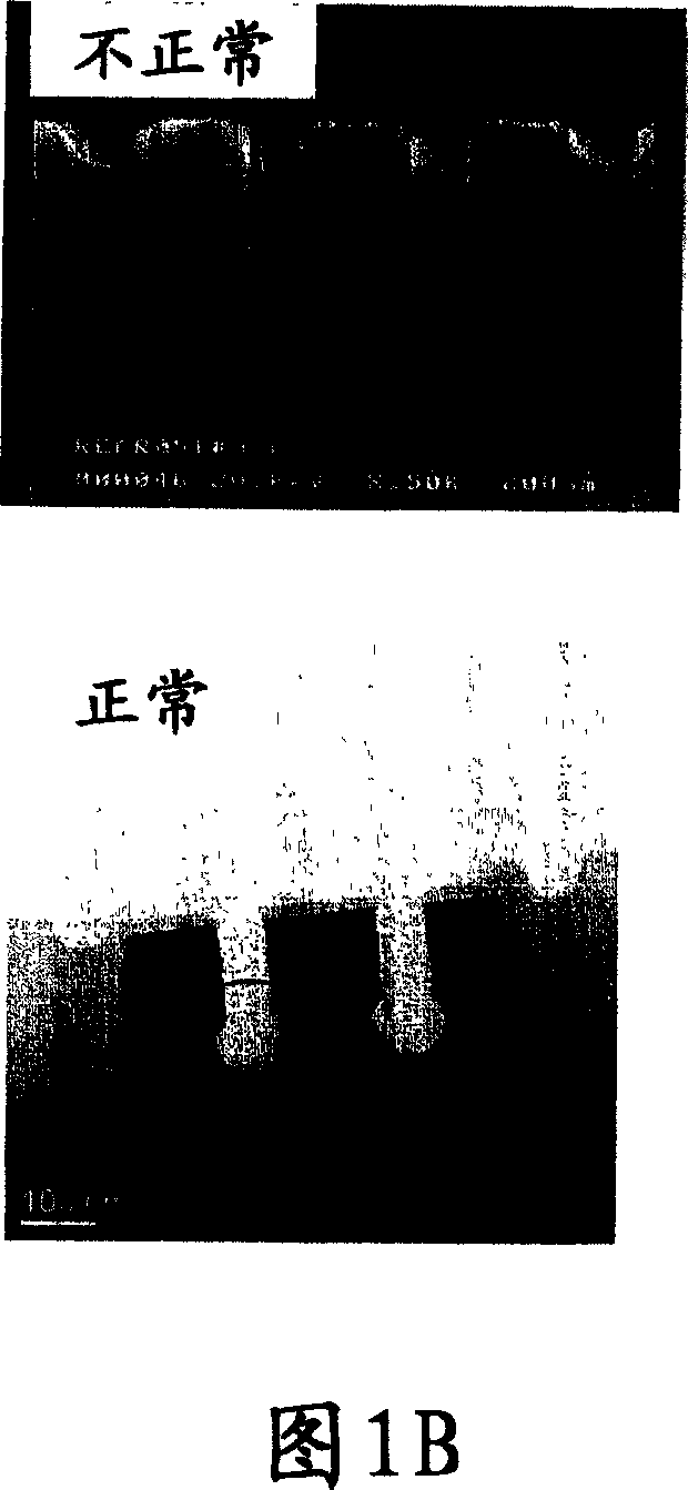
[0016] The present invention relates to a method of manufacturing a recessed channel with a highly reproducible ball pattern in a semiconductor device. When forming the recessed channel including the neck pattern and the ball pattern, the shape of the ball pattern can be precisely formed by controlling the etching process conditions for forming the ball pattern.

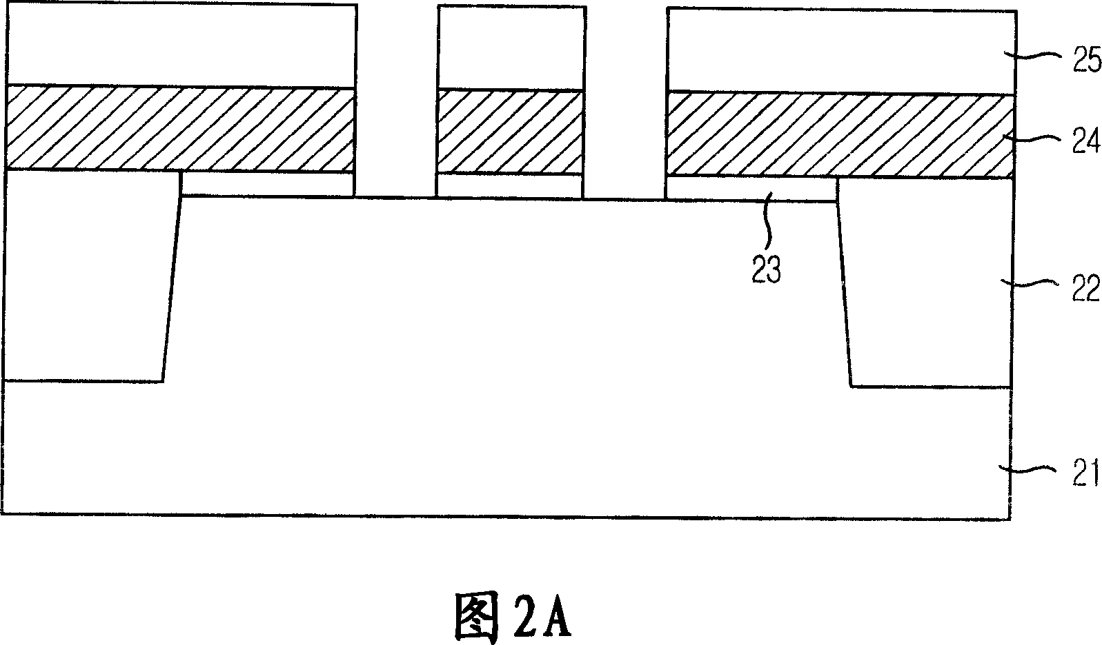
[0017] 2A-2F are schematic cross-sectional views of a method of making a recessed channel in accordance with certain embodiments of the present invention.

[0018] Referring to FIG. 2A , a device isolation structure 22 may be formed on a substrate 21 using a shallow trench isolation (STI) process. The device isolation structure 22 is filled in the trench. The trench has a depth of about 3000 Ȧ to about 4000 Ȧ.

[0019] As is well known, the STI process includes forming a pad oxide layer on the substrate 21 using a chemical vapor deposition (CVD) method. The pad oxide layer has a thickness of about 100 Ȧ to about 3...


PUM


Abstract

A method of fabricating a recess channel in a semiconductor device includes forming a hard mask pattern over a substrate, etching the substrate using the hard mask pattern to form first recesses, forming an insulation layer over the hard mask pattern and the first recesses, etching the insulation layer to form spacers on sidewalls of the first recesses and on sidewalls of the hard mask pattern, etching the substrate below the first recesses to form second recesses using a sulfur fluoride containing gas mixture, and removing the hard mask pattern and the spacers.

Description

[0001] Cross reference to related applications [0002] This application claims priority from Korean Patent Application No. 10-2006-0038786 filed on Apr. 28, 2006, which is hereby incorporated by reference in its entirety. technical field [0003] The present invention relates to a method of manufacturing a semiconductor device, more particularly, a method of manufacturing a recessed gate. Background technique [0004] In recent years, the pattern size of semiconductor devices of DRAM has gradually decreased, and the recessed gate process was introduced to overcome the short channel effect caused by the reduced channel length during gate formation in the cell region and to improve refresh characteristics, that is, the channel can be The region is recessed to a certain depth to form a recessed gate with a longer channel length. Typically, the recessed gate process includes forming a recessed channel by etching the recessed channel region of the substrate, and forming a gate ...

Claims


Application Information

Patent Timeline
Patent Type & Authority Applications(China)
IPC IPC(8): H01L21/308H01L21/28H01L21/336H01L21/822
CPCH01L21/3083H01L21/3081H01L27/10876H01L21/3065H01L21/31116H01L21/02057H10B12/053H01L21/18
Inventor 郑台愚
Owner SK HYNIX INC
Why Eureka
Try Eureka