
Method of fabricating a tunneling nanotube field effect transistor

A field effect transistor, nanotube technology, used in transistors, nanotechnology, nanotechnology, etc.

Active Publication Date: 2007-10-31
INT BUSINESS MASCH CORP +1
View PDF1 Cites 22 Cited by
  • Summary
  • Abstract
  • Description
  • Claims
  • Application Information

AI Technical Summary

Problems solved by technology

Too small a turn-on / turn-off current ratio prevents proper operation of digital circuits including these transistors and is therefore considered to be one of the main challenges in scaling the final device

Method used


Image

  • Method of fabricating a tunneling nanotube field effect transistor
  • Method of fabricating a tunneling nanotube field effect transistor
  • Method of fabricating a tunneling nanotube field effect transistor

Examples


Embodiment Construction

[0016] The present invention is a method of fabricating tunneling nanotube field effect transistors using selectively doped portions of nanotubes. Herein, the term "nanotube" is used interchangeably for nanotubes and nanowires (ie, nanotubes without axial openings). The method can be used to fabricate ultra-large scale integration (ULSI) circuits and devices.

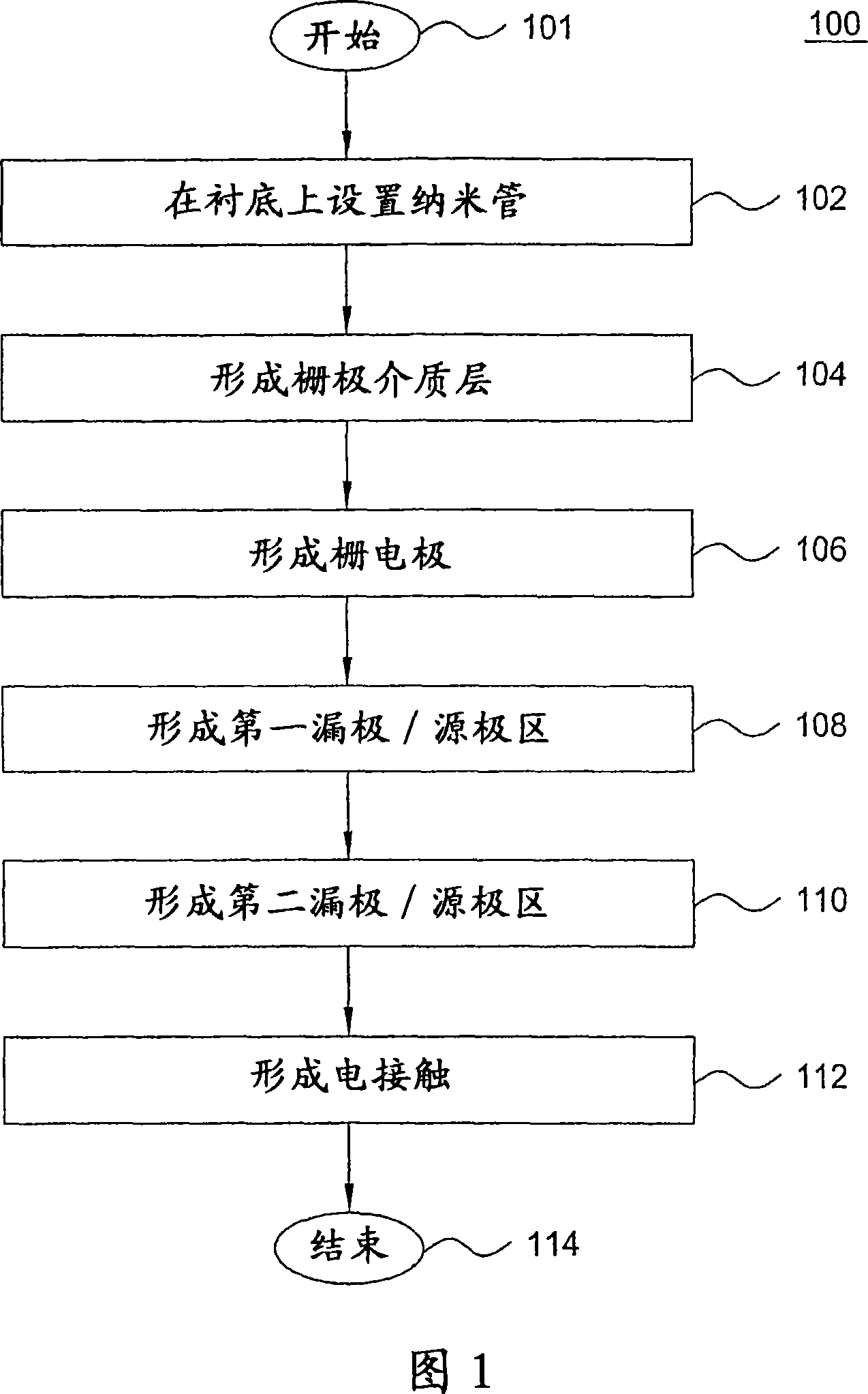
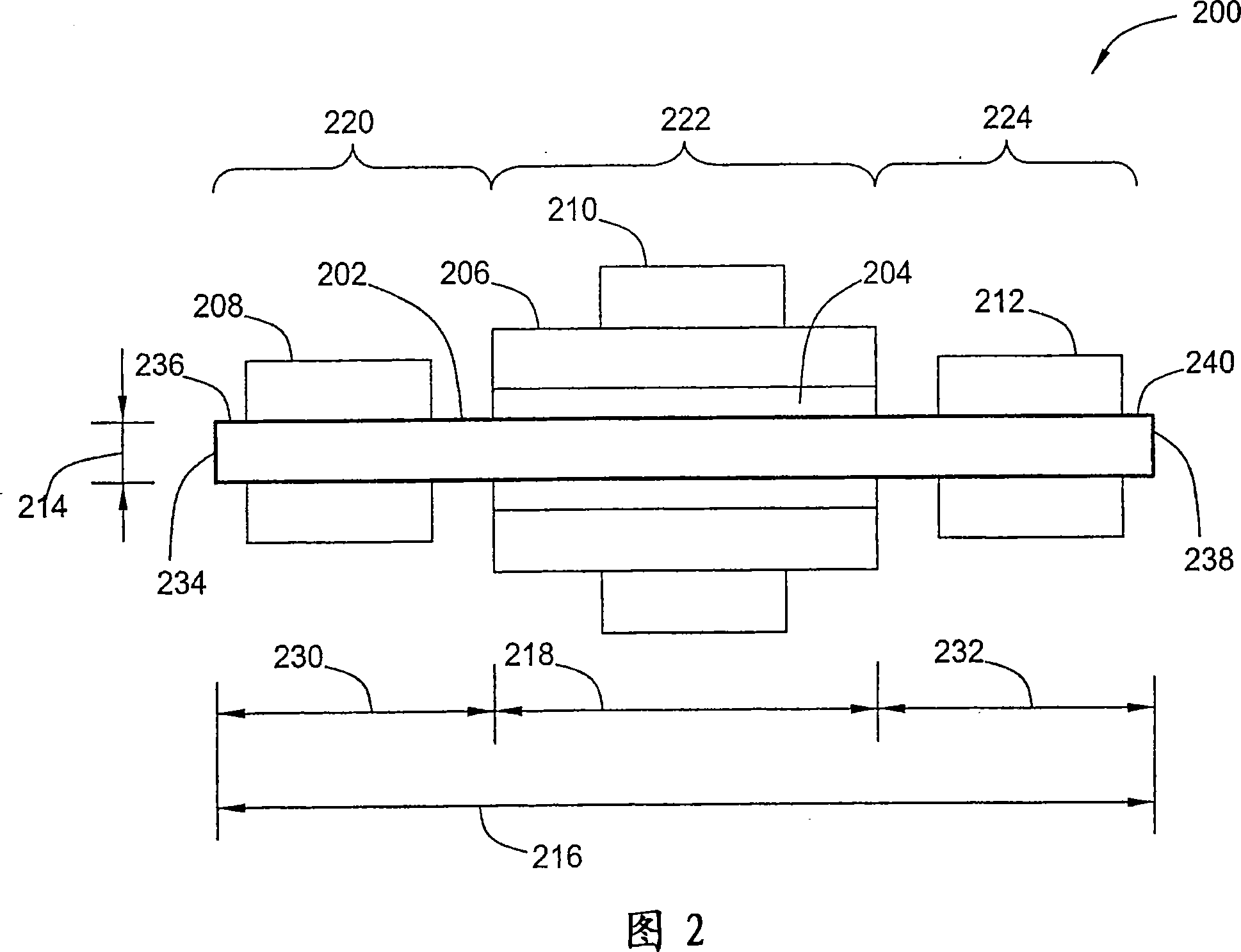
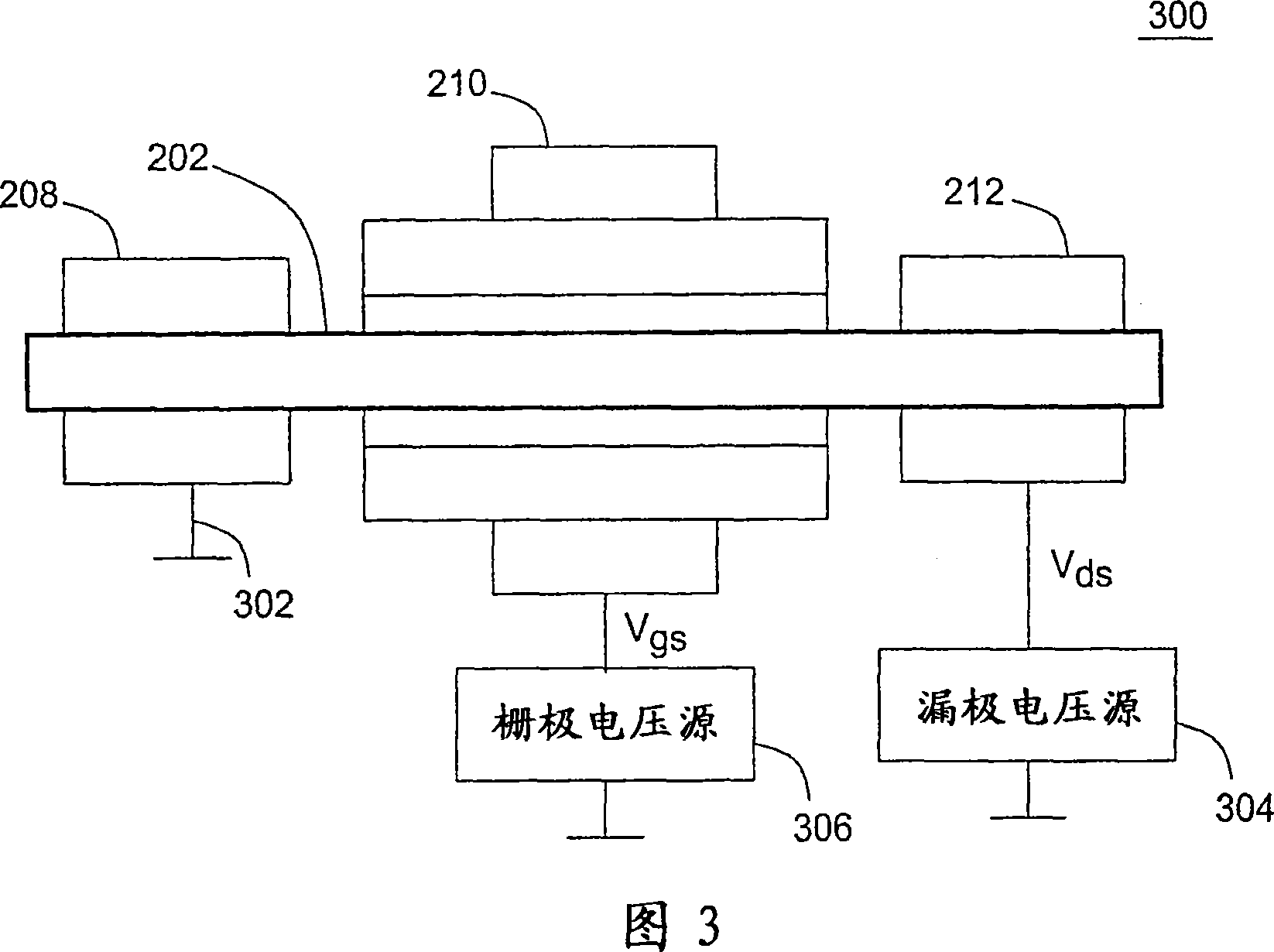
[0017] FIG. 1 shows a flowchart of one embodiment of a method of the present invention for fabricating a tunneling nanotube field effect transistor as method 100 . The method 100 includes processing steps performed on a substrate in which at least one tunneling nanotube field effect transistor is fabricated. In an exemplary embodiment, the processing steps are performed sequentially, in the order shown. In alternative embodiments, at least two processing steps may be performed simultaneously or in a different order. Conventional sub-processes such as application and removal of photolithographic masks or sacrificial a...


PUM

PropertyMeasurementUnit
diameteraaaaaaaaaa
diameteraaaaaaaaaa
lengthaaaaaaaaaa

Abstract

A method of fabricating a tunneling nanotube field effect transistor includes forming in a nanotube an n-doped region and a p-doped region which are separated by an undoped channel region of the transistor. Electrical contacts are provided for the doped regions and a gate electrode that is formed upon a gate dielectric layer deposited on at least a portion of the channel region of the transistor.

Description

technical field [0001] The present invention generally relates to methods of fabricating devices on semiconductor substrates. More specifically, the present invention relates to methods of fabricating tunneling nanotube field effect transistors on semiconductor substrates. Background technique [0002] Typically, microelectronic devices are fabricated on semiconductor substrates as integrated circuits. Complementary metal-oxide-semiconductor (CMOS) field-effect transistors are one of the core components in integrated circuits. In order to achieve higher performance and packing density of integrated circuits, the size and operating voltage of CMOS transistors are continuously reduced or scaled down. In particular, in such transistors the threshold voltage V th (that is, the voltage required to turn on the transistor) decreases. [0003] The switching characteristics of a CMOS transistor can be described by a parameter known in the art as the inverse sub-threshold slope, w...

Claims


Application Information

Patent Timeline
Patent Type & Authority Applications(China)
IPC IPC(8): H01B1/04H01L29/76H01L21/4763H01L29/06H01L29/739H01L29/80H01L29/88H10K99/00
CPCH01L51/0048Y10S977/734Y10S977/855Y10S977/815H01L51/0562Y10S977/742Y10S977/938H01L29/88Y10S977/755H01L29/0665Y10S977/749H01L29/0673H01L29/739B82Y10/00H01L51/0052H10K85/221H10K85/615H10K10/486
Inventor J·阿彭策勒J·克诺赫
Owner INT BUSINESS MASCH CORP
Learn More