
Image inspection device and image inspection method using the image inspection device

An image inspection and image technology, which is applied in the direction of measuring devices, instruments, semiconductor/solid-state device testing/measurement, etc., can solve problems such as inability to perform inspections, and achieve the effect of preventing light halos

Inactive Publication Date: 2007-11-14
MITSUBISHI ELECTRIC CORP
View PDF1 Cites 14 Cited by
  • Summary
  • Abstract
  • Description
  • Claims
  • Application Information

AI Technical Summary

Problems solved by technology

[0006] Conventional image inspection methods and image inspection apparatuses have a structure in which the peripheral portion of the object to be inspected is shielded by the device that clamps the object to be inspected as described above. Therefore, there is a problem that, when inspection is performed with transmitted light, due to the Passing light cannot pass through the covered part, so there is a part that cannot be inspected

Method used


Image

  • Image inspection device and image inspection method using the image inspection device
  • Image inspection device and image inspection method using the image inspection device
  • Image inspection device and image inspection method using the image inspection device

Examples


Embodiment approach 1

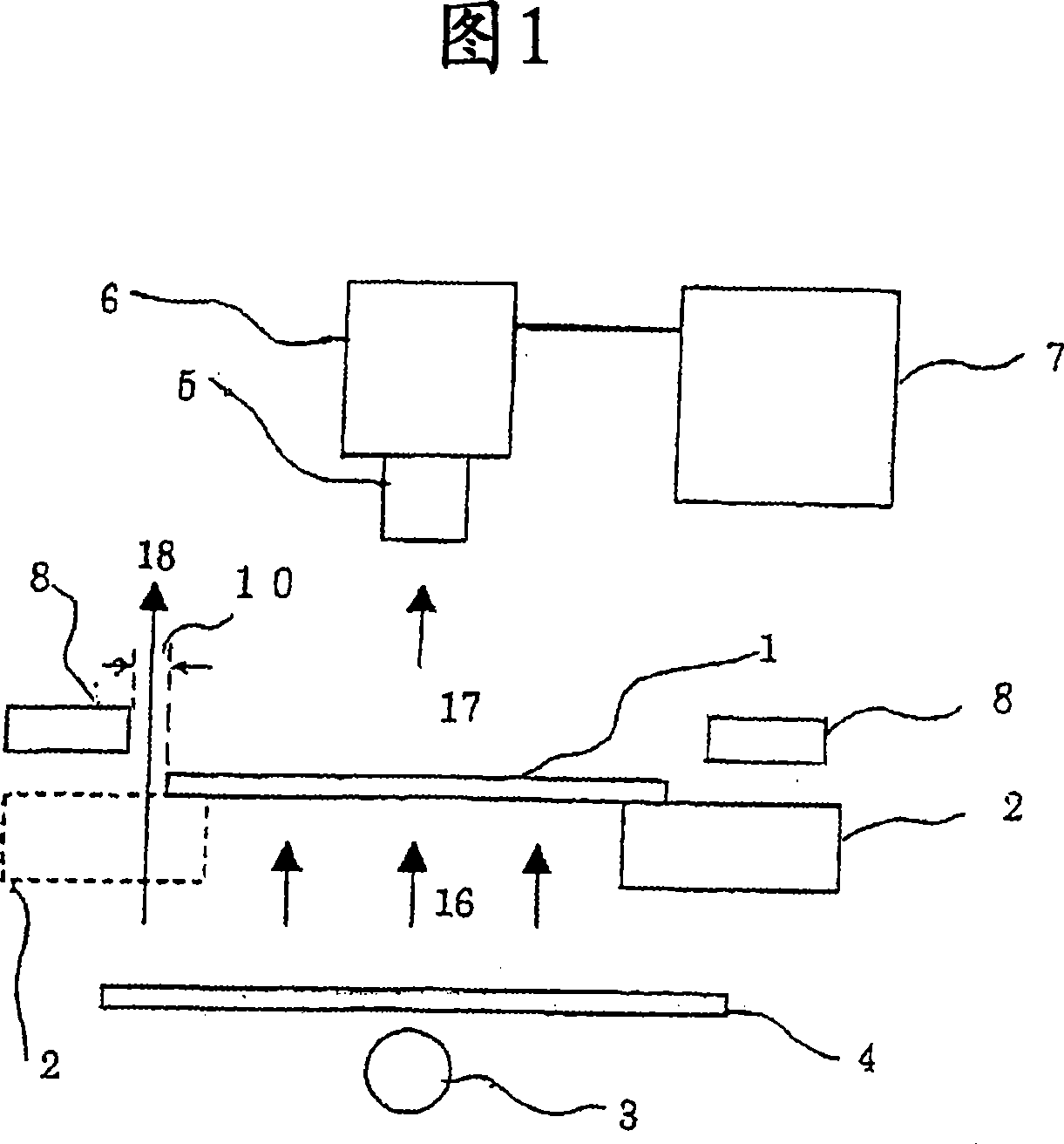
[0045] FIG. 1 is a configuration diagram showing Embodiment 1 of the present invention. In the figure, a holding table 2 holding a semiconductor wafer 1 (referred to as an inspection object holding mechanism) is provided below a semiconductor wafer 1 (an inspection object) that transmits infrared light. Here, the case where the semiconductor wafer 1 is quadrangular will be described. An infrared light source 3 is disposed below the semiconductor wafer 1 , and a plate of an infrared light diffuser 4 for diffusing infrared light is provided above the infrared light source 3 . Here, the infrared light diffuser 4 refers to a member having a function of uniformly diffusing infrared light, such as a translucent or frosted glass plate. For illustration, the infrared cursor emitted from the infrared light diffuser 4 is referenced 16 . The infrared light transmitted through the semiconductor wafer 1 is designated by reference numeral 17 . Above the semiconductor wafer 1, a camera 6 ...

Embodiment approach 2

[0059] In FIG. 1 of Embodiment 1, the mask 8 is shown as a plate-shaped member having a constant thickness. However, as shown in FIG. 6 , since the end face of the plate of the mask 8 is located at a position visible from the camera 6, the light emitted from the translucent object 4 may be reflected there (the reflected light is shown as 98 ) and may be emitted. into the camera. In order to solve this problem, as shown in FIG. 7 , a non-reflective mask 80 having a structure in which the end face is set as a sharp end portion 80a that is sharpened into a thin and sharp shape and has an inclined portion 80b such that No unwanted light is reflected in the direction of the semiconductor wafer 1 and the infrared camera 6 . Since the sharp end 80a is extremely thin, it will not be captured by the camera. In addition, since unnecessary reflected light is prevented from reaching the camera side by the inclined portion 80b, a better image can be obtained, and more stable crack inspec...

Embodiment approach 3

[0061] In Embodiment 1 and Embodiment 2, the example in which the infrared light diffuser 4 is installed horizontally was shown, but as shown in FIG. Infrared light diffuser4. By setting at a predetermined angle, dust or fragments of semiconductor wafers, etc. will not accumulate on the infrared light diffuser 4, thereby preventing dust and fragments accumulated on the translucent object 4 from being captured by the infrared camera 6. In this way, it is possible to eliminate erroneous confirmation of cracks and perform more stable crack inspection.


PUM


Abstract

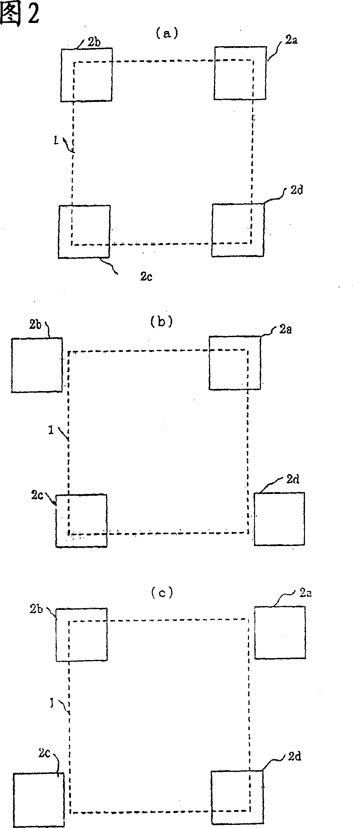
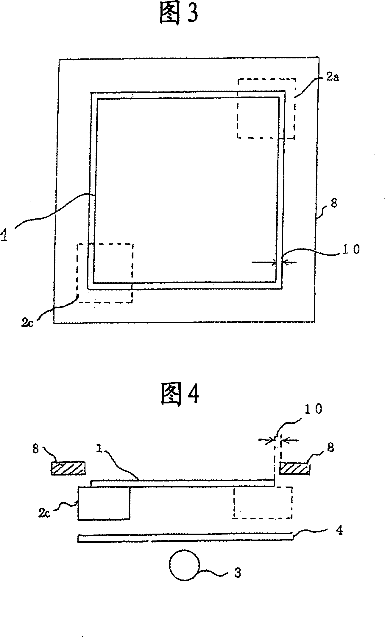
In an inspection of a semiconductor wafer for a defect, when infrared light passing through a semiconductor wafer is imaged by a camera and an inspection is conducted using the image, a problem that halation occurs in the camera due to light leaking from the side of the inspection object, which makes it impossible to conduct an inspection at the periphery portion occurs. An inspection object is irradiated by an infrared light source, and transmitted light is imaged by an infrared camera to be conducted. With the use of mask means that secures a clearance from the end portion on the outer side, it is possible to inspect on the peripheral portion. Also, as means for supporting the object, plural sets of those configured to be capable of evacuating are used, and by allowing the plural sets to evacuate alternately, it is possible to inspect across the entire surface.

Description

technical field [0001] The present invention relates to an image inspection method and an improvement of an image inspection device for taking an image of a plate-shaped object to be inspected such as a semiconductor wafer through which infrared light is transmitted, and inspecting defects from the image. Background technique [0002] There is a device for inspecting defects (cracks or adhesion of foreign matter) in plate-shaped transparent or translucent objects such as semiconductor wafers and liquid crystal panels. In the description of the present invention, the case of a semiconductor wafer is described for convenience of description, but the application object of the present invention is not limited to a semiconductor wafer (it may also be called a cell). For example, Patent Document 1 discloses an inspection device that detects cracks in a semiconductor wafer by irradiating infrared rays on a semiconductor crystal as an object to be inspected. In Fig. 1 of Patent Doc...

Claims


Application Information

Patent Timeline
Patent Type & Authority Applications(China)
IPC IPC(8): G01N21/958H01L21/66
CPCG01N21/9505G01N21/9503
Inventor 西野裕久小原隆雄宇野真彦
Owner MITSUBISHI ELECTRIC CORP
Learn More