Inspection device and inspection method

a technology of inspection device and inspection method, which is applied in the direction of reference comparison, automatic balancing arrangement, instruments, etc., can solve the problems of increasing the number of inspection steps, the conductor of testing cannot uniformly come into contact with the panel surface, and the touch sensitivity of the panel deteriorates, etc., to achieve the effect of stable inspection on the performance of the touch panel

Active Publication Date: 2020-06-30
SHARP KK
View PDF4 Cites 0 Cited by
  • Summary
  • Abstract
  • Description
  • Claims
  • Application Information

AI Technical Summary

Benefits of technology

[0013]According to an aspect of the present invention, it is possible to carry out stable inspection on performance of a touch panel.

Problems solved by technology

In this type of panel, in a case where a resistance value of the transparent film becomes smaller than a normal value, a touch signal becomes weaker and consequently, touch sensitivity of the panel deteriorates.
According to the above method, however, it is likely that the number of inspection steps increases and the testing conductor cannot uniformly come into contact with the panel surface.
This disadvantageously leads to unstable inspection and hinders accurate inspection.
There is another concern that, for example, the panel surface may be scratched due to contact with the testing conductor.

Method used


Image

  • Inspection device and inspection method
  • Inspection device and inspection method

Examples


embodiment 1

[0018]The following description will discuss, in detail, Embodiment 1 of the present invention.

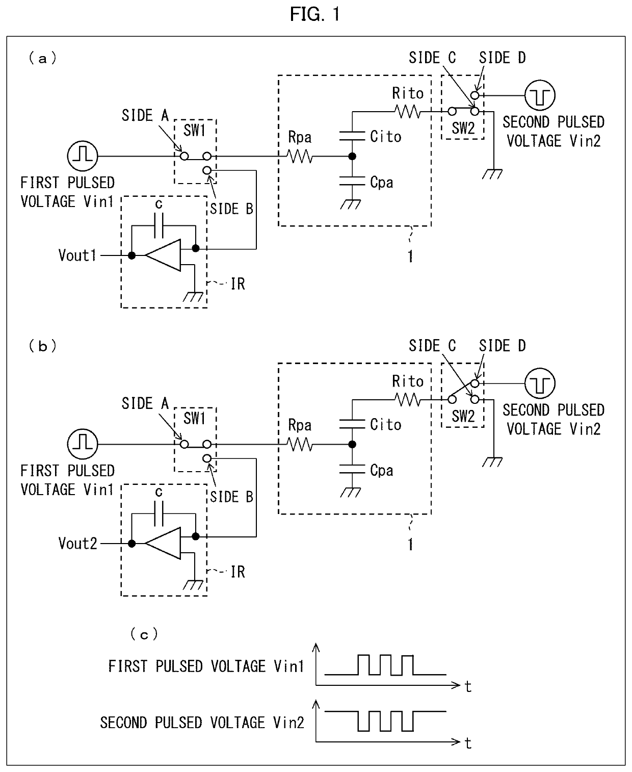
[0019]FIG. 1 illustrates a touch panel 1 of Embodiment 1 and a configuration of its peripheral circuit. (a) of FIG. 1 illustrates a circuit configuration employed in a first measurement step. (b) of FIG. 1 illustrates a circuit configuration employed in a second measurement step. (c) of FIG. 1 is a waveform chart illustrating waveforms of a first pulsed voltage Vin1 and a second pulsed voltage Vin2.

[0020]In an inspection method for inspecting the touch panel 1 on the basis of a resistance value of a transparent film 11 of the touch panel 1, which includes at least the transparent film 11, a CF glass (dielectric member) 12, and a TP sensor (sensor) 13 stacked on top of each other, the inspection method includes the steps of: obtaining a first background capacitance of the touch panel 1 by applying a first pulsed voltage to the TP sensor 13 in such a state that the transparent film 11 is con...

embodiment 2

[0053]The following description will discuss Embodiment 2 of the present invention. For convenience, the same reference signs will be given to members having the same functions as those of Embodiment 1, and their descriptions will be omitted.

[0054]Note that it is preferred to carry out inspection on performance of a touch panel 1 in a state prior to mounting the touch panel 1 to a module. This is because, in a case where inspection on performance of the touch panel is carried out by using a product (module) including the touch panel and then a resistance value of the transparent film 11 is found to be small, members mounted on the module may be useless.

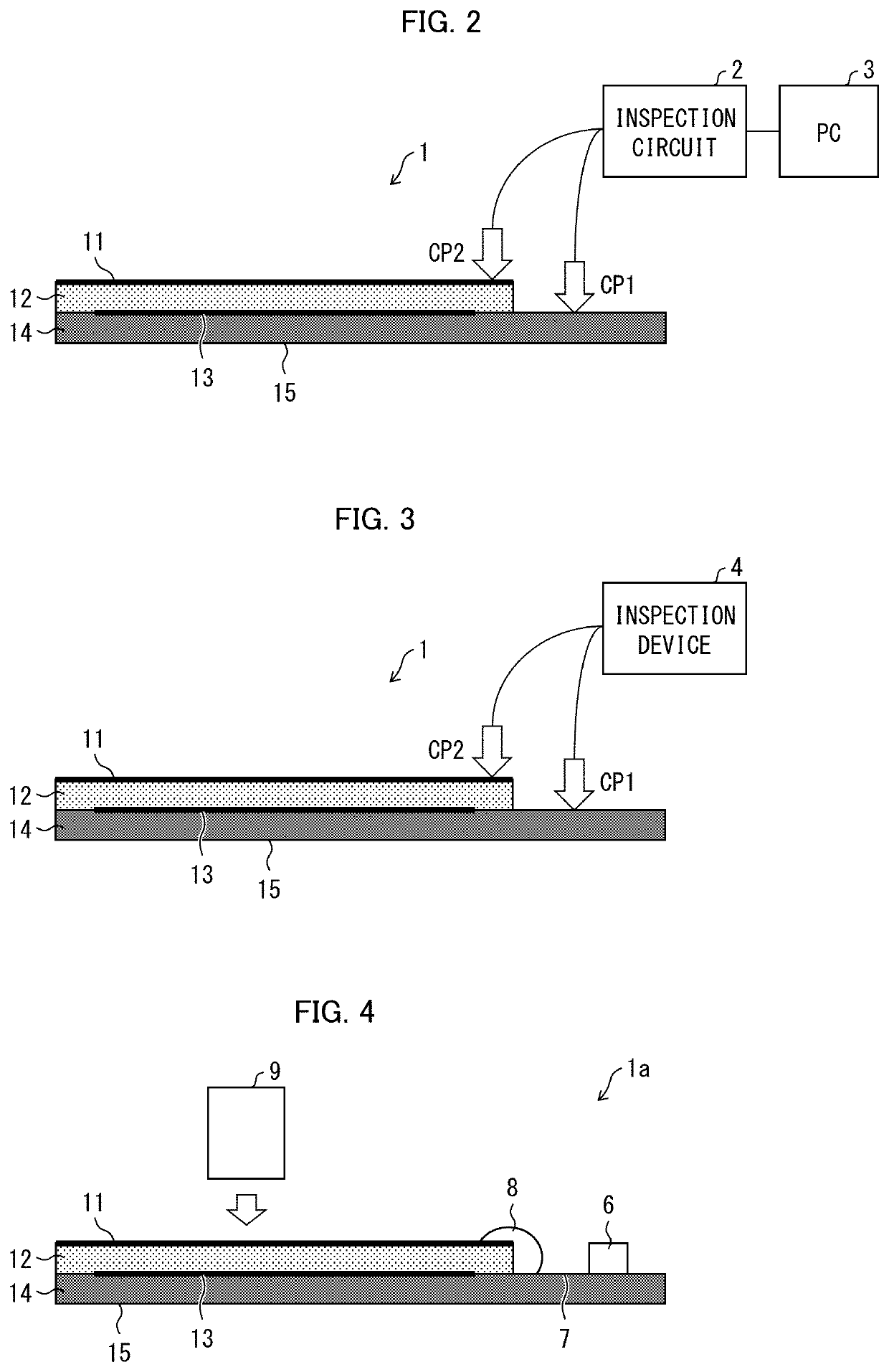
[0055]FIG. 2 illustrates a touch panel 1 and an inspection device in accordance with Embodiment 2. The touch panel 1 includes a transparent film 11, a CF glass 12, a TP sensor 13, a liquid crystal layer 14, and a TFT glass 15, which are stacked on top of each other.

[0056]The touch panel 1 has a terminal provided on the surface of the ...

embodiment 3

[0059]The following description will discuss Embodiment 3 of the present invention. For convenience, the same reference signs will be given to members having the same functions as those of Embodiments 1 and 2, and their descriptions will be omitted.

[0060]Whereas Embodiment 2 describes an example case employing a PC 3 dedicated to inspection, Embodiment 3 describes an example case where a PC is not employed.

[0061]In an inspection device 4 for inspecting a touch panel 1 on the basis of a resistance value of a transparent film 11 of the touch panel 1, which includes at least the transparent film 11, a CF glass 12, and a TP sensor 13 stacked on top of each other, the inspection device 4 includes: a background capacitance obtaining section configured to obtain a background capacitance of the touch panel 1 by applying a first pulsed voltage Vin1 to the TP sensor 13; and a switch (switching section) SW2 configured to connect the transparent film 11 to a ground or to a generator circuit (ge...


PUM

PropertyMeasurementUnit
resistance valueaaaaaaaaaa
transparentaaaaaaaaaa
capacitanceaaaaaaaaaa

Abstract

An embodiment of the present invention makes it possible to carry out stable inspection on performance of a touch panel. An inspection device for inspecting a touch panel on a basis of a resistance value of a transparent film of the touch panel, which includes at least the transparent film, a dielectric member, and a sensor stacked on top of each other, includes: an integrating circuit configured to obtain a background capacitance of the touch panel by applying a first pulsed voltage to the sensor; and a switch configured to connect the transparent film to a ground or to a generator configured to generate a second pulsed voltage which is opposite in phase to the first pulsed voltage.

Description

[0001]This Nonprovisional application claims priority under 35 U.S.C. § 119 on Patent Application No. 2018-071589 filed in Japan on Apr. 3, 2018, the entire contents of which are hereby incorporated by reference.TECHNICAL FIELD[0002]The present invention relates to an inspection device and an inspection method.BACKGROUND ART[0003]A currently available full-in-cell touch panel has a surface on which a high-resistance transparent film is formed. In this type of panel, in a case where a resistance value of the transparent film becomes smaller than a normal value, a touch signal becomes weaker and consequently, touch sensitivity of the panel deteriorates.[0004]Such deterioration in touch sensitivity of the touch panel can be detected, for example, by checking whether or not a signal value is not smaller than a predetermined value in a case where a testing conductor brought into contact with a panel surface is slid over the panel surface. According to the above method, however, it is lik...

Claims


Application Information

Patent Timeline
Patent Type & Authority Patents(United States)
IPC IPC(8): G01R27/26G06F3/041G06F3/044G01R17/02G01R17/00
CPCG01R17/02G01R27/26G01R27/2605G06F3/0416G06F3/044G01R17/00G06F2203/04106G01R27/02G06F3/041G06F3/0418G06F11/2221
Inventor HOSHIAI, NORIYUKIMIYAZAKI, SHINICHI
Owner SHARP KK
Why Eureka
Try Eureka