

Semiconductor packaging structure and method for making the same
A technology for semiconductors and manufacturing methods, applied in the field of semiconductor packaging structures and manufacturing methods, can solve problems such as reducing product circuit layout and reliability, increasing manufacturing process equipment cost and complexity, etc., to improve circuit layout and reliability, The effect of improving accuracy and success rate
- Summary
- Abstract
- Description
- Claims
- Application Information
AI Technical Summary
Problems solved by technology
Method used
Image

Examples
no. 1 example
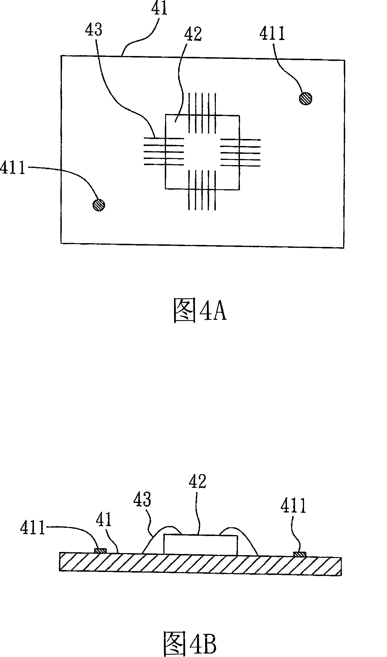
[0062] Referring to FIGS. 4A to 4H , they are schematic diagrams of a first embodiment of the semiconductor assembly structure and its manufacturing method of the present invention.
[0063] As shown in Figures 4A and 4B, a substrate 41 is provided, and the substrate 41 is provided with an identification point 411, and the identification point 411 can be a dot, which can be formed on the substrate 41 by electroplating a metal layer, preferably in the form of The identification point is formed by electroplating gold. In addition, a semiconductor chip 42 is mounted on the substrate 41 , and the semiconductor chip 42 is electrically connected to the substrate 41 by gold wires 43 . In addition, the semiconductor chip 42 can also be mounted in a flip-chip manner and electrically connected to the substrate 41 .
[0064] As shown in Figures 4C and 4D, a heat sink 44 is provided at the same time, the heat sink 44 includes a flat portion 442, and a support portion 441 integrally conne...
no. 2 example
[0068] Referring to FIG. 5 , it is a schematic diagram of a second embodiment of the present invention.
PUM
 Abstract
Description
Claims
Application Information