
Semiconductor device and its making method

A manufacturing method and semiconductor technology, applied in the direction of semiconductor/solid-state device manufacturing, semiconductor devices, semiconductor/solid-state device components, etc., can solve problems such as weak connection strength, increased manufacturing costs and difficulties of semiconductor devices, and achieve accurate photosensitive or Effects of imaging, improvement of in-plane uniformity, and increase in manufacturing cost

Inactive Publication Date: 2008-01-09
SANYO ELECTRIC CO LTD
View PDF1 Cites 9 Cited by
  • Summary
  • Abstract
  • Description
  • Claims
  • Application Information

AI Technical Summary

Problems solved by technology

However, since it is extremely difficult to perform the grinding uniformly, the in-plane uniformity of the back surface of the thin film portion 210T thinned by the grinding is lowered.
Therefore, the light incident on the thin film portion 210T is deflected, and imaging unevenness occurs when the CCD receives light, that is, captures images.
That is, the performance of the semiconductor device is degraded
In addition, since the cost of local thinning of such a semiconductor substrate is high, the manufacturing cost of the semiconductor device is increased.
[0010] In addition, after the semiconductor device is completed, the mechanical strength of the thin film portion 210T of the semiconductor chip 210 is weak.
In addition, the connection strength of the protrusion 216 that electrically connects the semiconductor chip 210 and the support body 215 is also weak.
Therefore, the electrical connection between elements or electrodes is likely to become insufficient, and as a result, the performance of the semiconductor device is degraded.

Method used


Image

  • Semiconductor device and its making method
  • Semiconductor device and its making method
  • Semiconductor device and its making method

Examples


Embodiment Construction

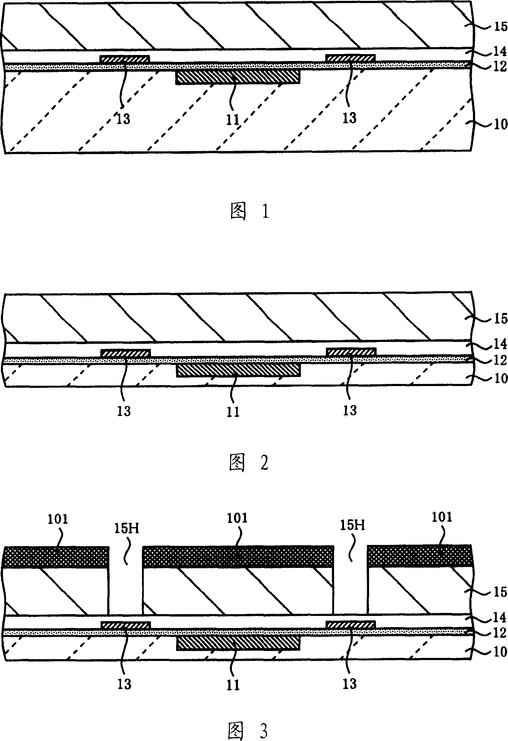
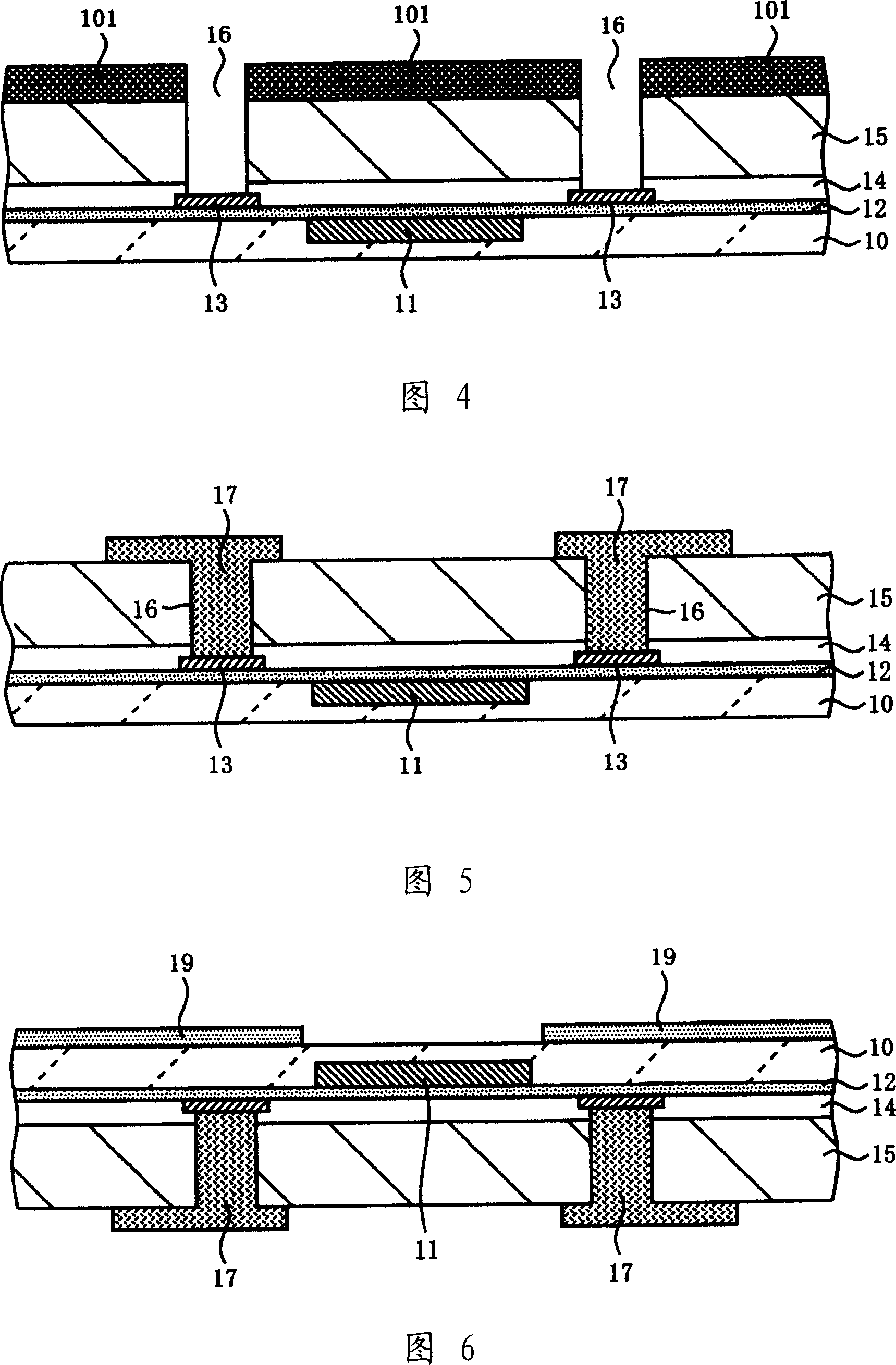
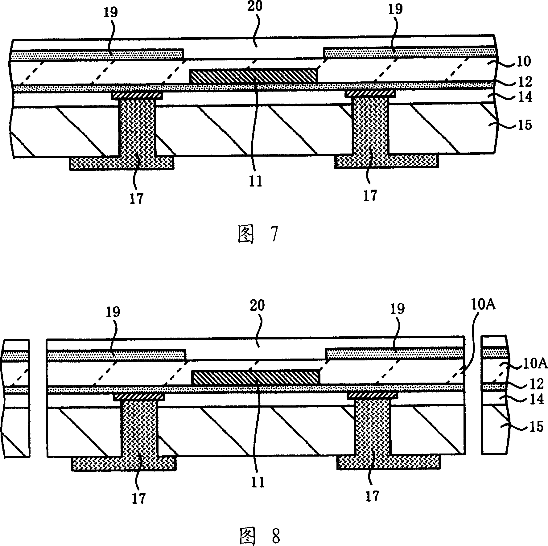
[0028] Next, a semiconductor device according to an embodiment of the present invention will be described with reference to the drawings. The manufacturing method of the semiconductor device of this embodiment is performed as follows, for example. 1 to 8 are cross-sectional views illustrating a method of manufacturing a semiconductor device according to this embodiment. In addition, FIG. 9 is a cross-sectional view illustrating the semiconductor device and its manufacturing method according to the present embodiment.

[0029] In addition, FIGS. 1 to 9 show cross-sections of semiconductor substrates at predetermined adjacent chip boundaries (that is, near scribe lines not shown) separated by a dicing process described later.

[0030] First, as shown in FIG. 1 , a photosensitive element such as a CCD (Charge Coupled Device) is formed on the surface of a semiconductor substrate 10 made of a silicon substrate as a photosensitive element. The CCD 11 is not particularly limited, b...


PUM


Abstract

The invention is concerned with the back injection semiconductor with the sensitization component. It is to stick the supporting body (-) on the surface of the semiconductor plaque (-) that has the sensitization component (-) and its bonding pad electrode (-). Next, it is to etch the supporting body (-) to form the pin-through-hole (-) that run-through the supporting body (-) but show up the bonding pad electrode (-). Then, it is to form the wiring (-) extending on the surface of the supporting body (-), through the pin-through-hole (-) and connecting the bonding pad electrode (-). At the last, it is to apart the semiconductor plaque (-) into several of the semiconductor chip (-) through slotting. The semiconductor makes the supporting body (-) and the circuitry plaque (-) face to face to conduct the installation.

Description

technical field [0001] The present invention relates to a semiconductor device and a manufacturing method thereof, and in particular, to a back-illuminated semiconductor device mounted with a photosensitive element and a manufacturing method thereof. Background technique [0002] Conventionally, among semiconductor devices on which a photosensitive element is mounted, a semiconductor device that detects light incident from a main surface of a semiconductor chip opposite to a surface on which the photosensitive element is formed is known. Such semiconductor devices are called back-illuminated or back-illuminated semiconductor devices. Next, the configuration of a conventional example of a back-illuminated semiconductor device will be described with reference to the drawings. FIG. 10 is a cross-sectional view illustrating a conventional semiconductor device. [0003] As shown in FIG. 10 , a CCD (Charge Coupled Device) 221 as a photosensitive element and its pad electrode 213...

Claims


Application Information

Patent Timeline
Patent Type & Authority Applications(China)
IPC IPC(8): H01L27/14H01L27/148H01L23/48H01L21/82H01L21/60
CPCH01L2224/10H01L2224/48091H01L2224/73204H01L2224/73265
Inventor 野间崇
Owner SANYO ELECTRIC CO LTD
Learn More