Nonvolatile semiconductor storage device and method for operating same

A storage device, non-volatile technology, applied in information storage, static memory, read-only memory, etc.

Active Publication Date: 2008-01-23
异基因开发有限责任公司
View PDF2 Cites 14 Cited by
  • Summary
  • Abstract
  • Description
  • Claims
  • Application Information

AI Technical Summary

Problems solved by technology

However, even when a precharge period is provided before transitioning to each operation, similar to the case of directly transitioning between reading, writing, and erasing

Method used


Image

  • Nonvolatile semiconductor storage device and method for operating same
  • Nonvolatile semiconductor storage device and method for operating same
  • Nonvolatile semiconductor storage device and method for operating same

Examples


no. 1 approach

[0071] First, referring to FIG. 8 to FIG. 14, the common non-selection voltage V WE / 2 is given for the first embodiment of the unselected word line and the unselected bit line.

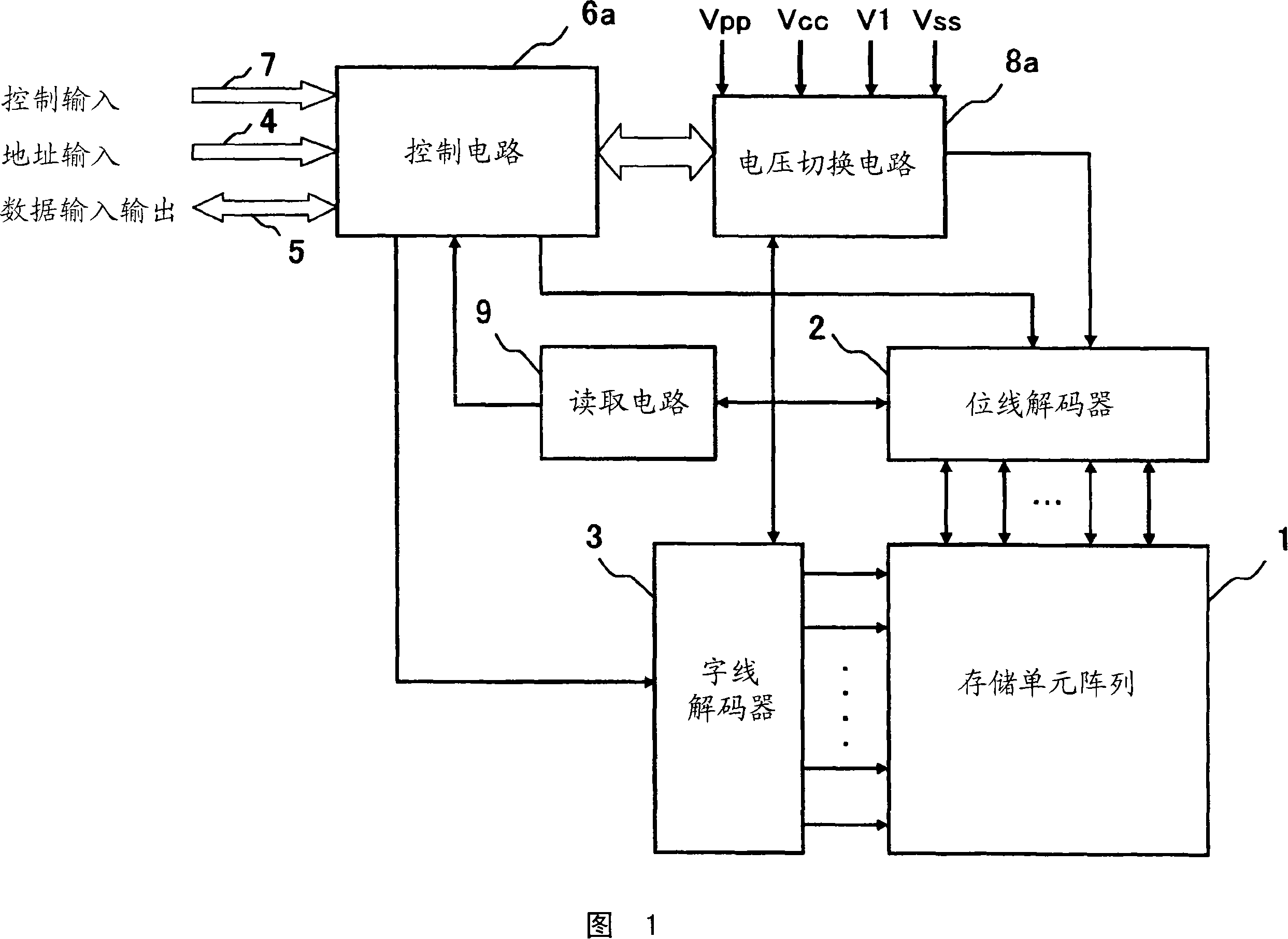
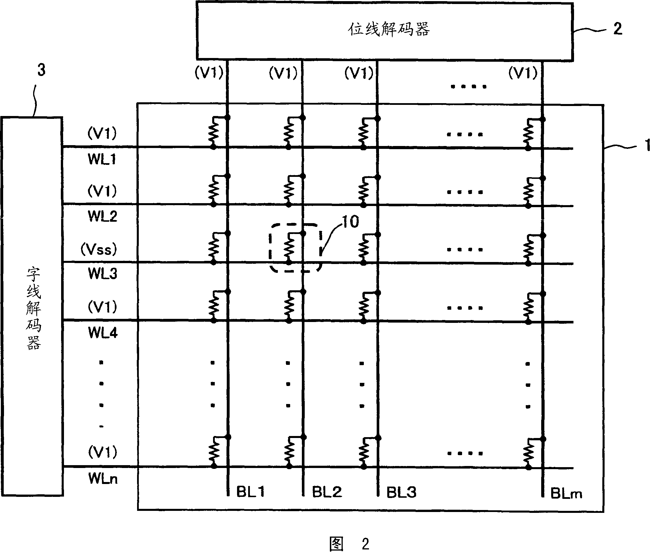
[0072] Fig. 8 is a block configuration diagram showing the functional configuration of the device of the present invention. In FIG. 8 , common reference numerals are assigned to common parts with conventional nonvolatile semiconductor memory devices. As shown in FIG. 8, for the device of the present invention, the memory cell array 1 in which the 1R-type memory cells are arranged in a matrix illustrated in FIG. 9 has a bit line decoder 2, a word line decoder 3, and a voltage switching circuit 8d around , the reading circuit 9 and the control circuit 6d. Basically, it has the same structure as the conventional nonvolatile semiconductor memory device shown in FIG. 1 . The difference from the structure of the conventional nonvolatile semiconductor memory device shown in FIG. 1 is that the voltages ap...

no. 2 approach

[0088] Next, referring to FIG. 15 to FIG. 21 , the first method of providing the ground voltage Vss as a common non-selected voltage to the non-selected word line and the non-selected bit line in each storage operation of writing, erasing, and reading of the device of the present invention is described. Two implementation modes.

[0089] Fig. 15 is a block configuration diagram showing the functional configuration of the device of the present invention according to the second embodiment. In FIG. 15 , the parts common to the conventional nonvolatile semiconductor memory device and the first embodiment are denoted by common reference numerals and described. As shown in FIG. 15, for the device of the present invention, the memory cell array 1 in which the 1R-type memory cells are arranged in a matrix illustrated in FIG. 16 has a bit line decoder 2, a word line decoder 3, and a voltage switching circuit 8e around , the reading circuit 9 and the control circuit 6e. The structure ...

no. 3 approach

[0102] Then, with reference to FIG. 22 to FIG. 28 , it is explained that in each storage operation of writing, erasing, and reading of the device of the present invention, the writing voltage V is provided to the non-selected word line and the non-selected bit line. WE 1 / 3 of the common first non-selection voltage V WE / 3 of the third embodiment.

[0103] Fig. 22 is a block configuration diagram showing the functional configuration of the device of the present invention according to the third embodiment. In FIG. 22 , the parts common to the conventional nonvolatile semiconductor memory device and the first embodiment are denoted by common reference numerals and described. As shown in FIG. 22, for the device of the present invention, a bit line decoder 2, a word line decoder 3, a voltage switching circuit 8f, Read circuit 9 and control circuit 6f. The structure is basically the same as that of the conventional nonvolatile semiconductor memory device shown in FIG. 1 and the f...


PUM


Abstract

A nonvolatile semiconductor storage device provided with a highly integrated memory cell array wherein consumption current increase caused by a transient current due to potential change of a bit line and a word line is suppressed during shifts among modes of reading, writing and erasing. A two-terminal memory cell is provided with a variable resistance element whose resistance value reversibly changes by pulse application. In the memory cell array (1), a plurality of two-terminal memory cells are arranged in a row direction and a column direction, respectively, and ends on one side of the memory cells on a same row are connected to common word lines (WL1-WLn), and the other ends of the memory cells on a same column are connected to common bit lines (BL1-BLm). While the operation of reading, writing and erasing are performed to a selective memory cell, a common nonselective voltage VWE/2 is applied to both a nonselective word line and a nonselective bit line not connected to the selective memory cell.

Description

technical field [0001] The present invention relates to a semiconductor memory device having a memory cell array in which a plurality of two-terminal memory cells are arranged in a row direction and a column direction respectively, and the two-terminal memory cells have a resistance value reversibly changed by application of an electric pulse, and A variable resistive element that stores information according to changes in resistance. More specifically, the present invention relates to the voltage control technology of bit lines and word lines for each storage operation of reading, writing, and erasing operations of a memory cell array. Background technique [0002] In recent years, as a next-generation non-volatile random access memory (NVRAM: Nonvolatile Random Access Memory) that can replace flash memory and can operate at high speed, various types such as FeRAM (Ferroelectric RAM), MRAM (Magnetic RAM), and OUM (Ovonic Unified Memory) have been proposed. Device structure,...

Claims


Application Information

Patent Timeline
IPC IPC(8): G11C13/00
CPCG11C2213/31G11C13/0007G11C5/063G11C16/10G11C16/26G11C13/0002G11C13/0021G11C13/004G11C13/0069
Inventor 川添豪哉玉井幸夫
Owner 异基因开发有限责任公司
Why Eureka
Try Eureka