Integrated circuit package structure and anti-warp substrates

An integrated circuit and structural technology, applied in circuits, electrical components, electrical solid devices, etc., can solve the problems affecting cutting efficiency, general products have no structure, inconvenience, etc., and achieve the effect of enhancing structural strength and improving anti-warping performance.

Inactive Publication Date: 2008-01-30
POWERTECH TECHNOLOGY
View PDF2 Cites 6 Cited by
  • Summary
  • Abstract
  • Description
  • Claims
  • Application Information

AI Technical Summary

Problems solved by technology

However, the reinforcing member is an additional component and occupies a certain area on the lower surface of the substrate. When it is within the unit area, it will affect the setting space of its external terminals, and when it is outside the unit area, it will affect the cutting efficiency.
[0009] It can be seen that the above-mentioned existing integrated circuit packaging structure obviously still has inconvenience

Method used


Image

  • Integrated circuit package structure and anti-warp substrates
  • Integrated circuit package structure and anti-warp substrates
  • Integrated circuit package structure and anti-warp substrates

Examples


Embodiment Construction

[0102] In order to further explain the technical means and effects that the present invention adopts to achieve the intended invention purpose, the specific implementation, structure, features and effects of the integrated circuit packaging structure proposed according to the present invention will be described below in conjunction with the accompanying drawings and preferred embodiments. , as detailed below.

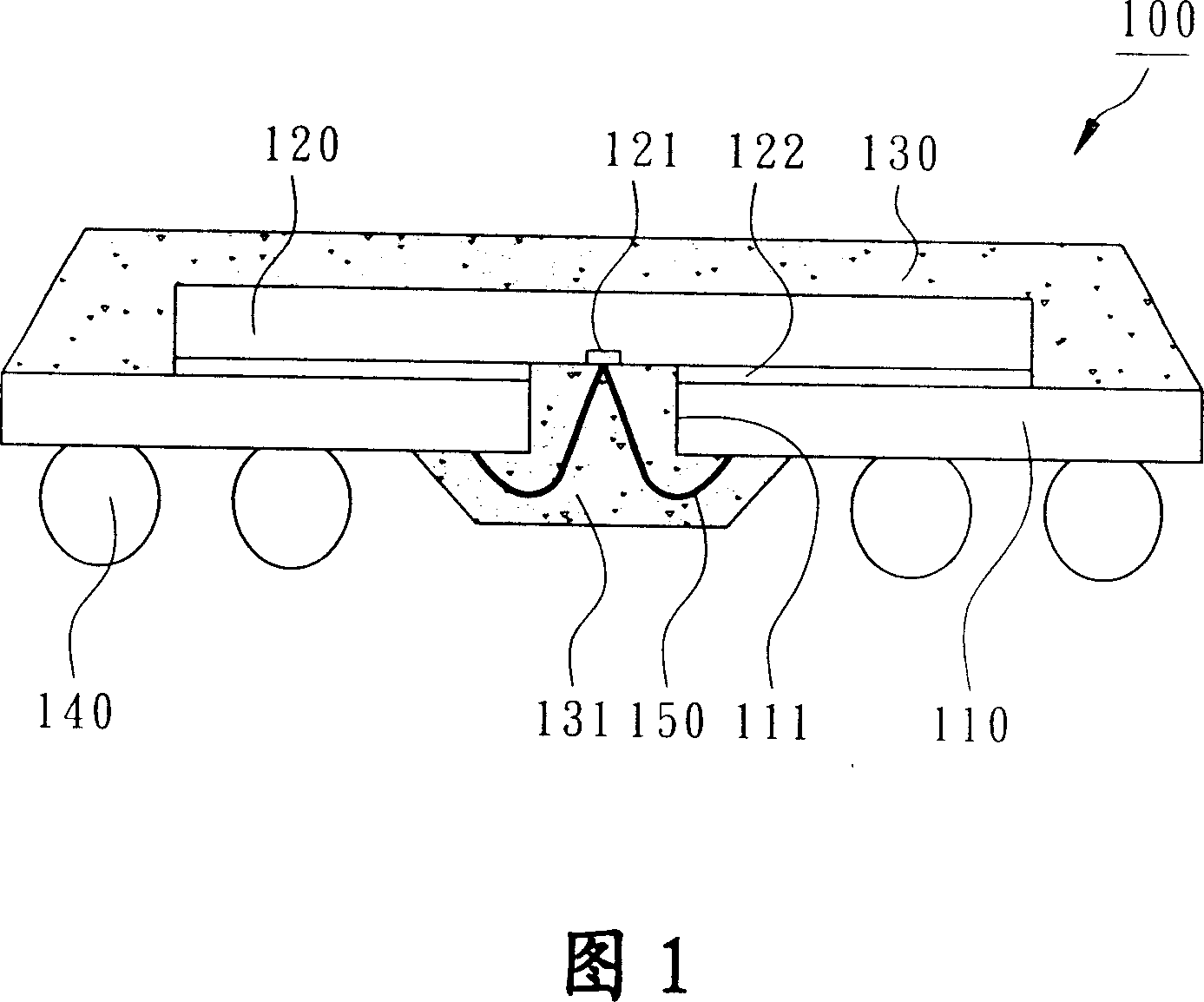
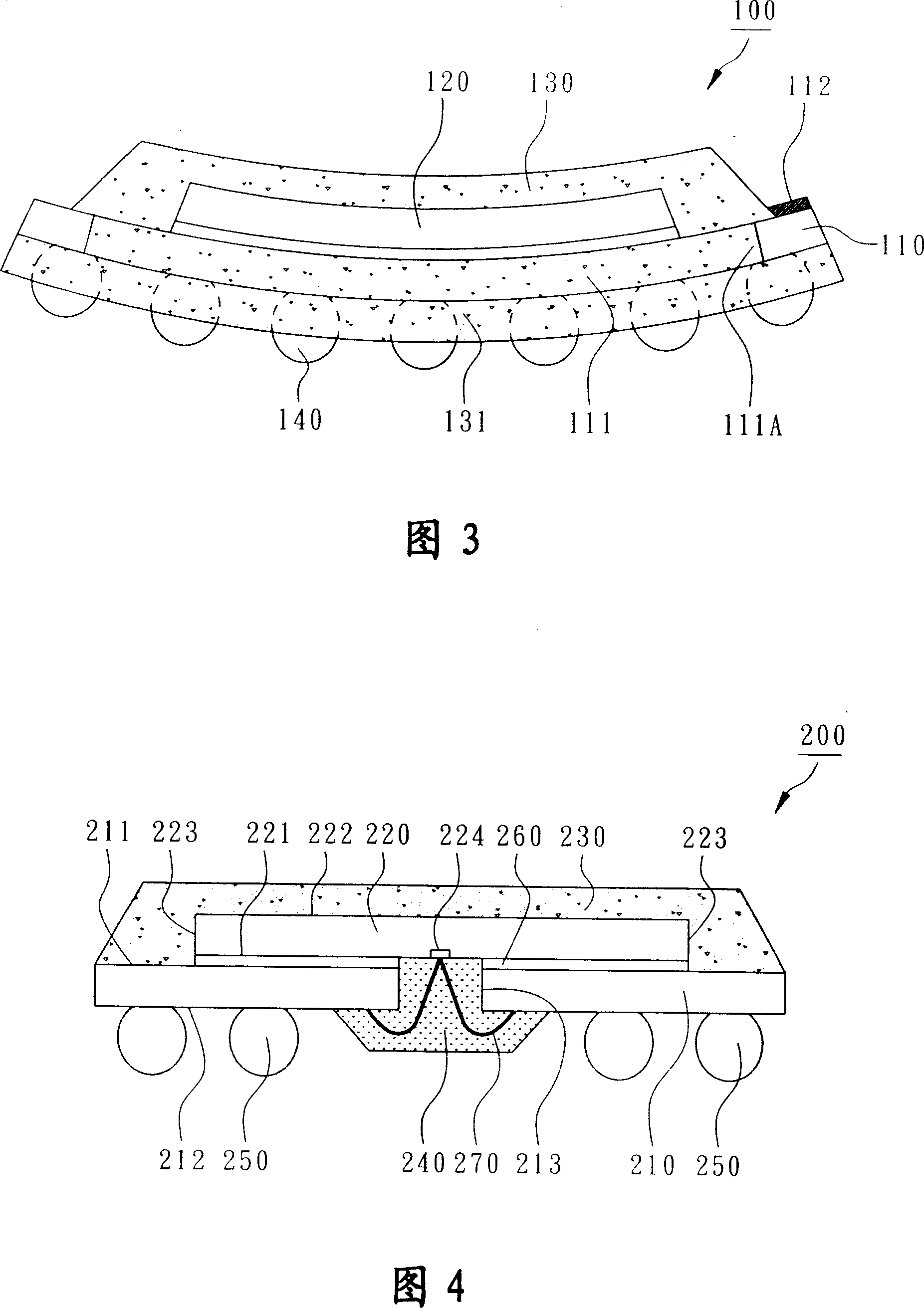
[0103] Please refer to FIG. 4 to FIG. 8 , which are related to the first specific embodiment of the present invention, which discloses an integrated circuit packaging structure. The integrated circuit packaging structure 200 can be a window type ball grid array package (Window BGA package), mainly including a substrate 210, a chip 220, a covering molding body 230, at least one reinforcing type molding body 240 and a plurality of external connections. Terminal 250.

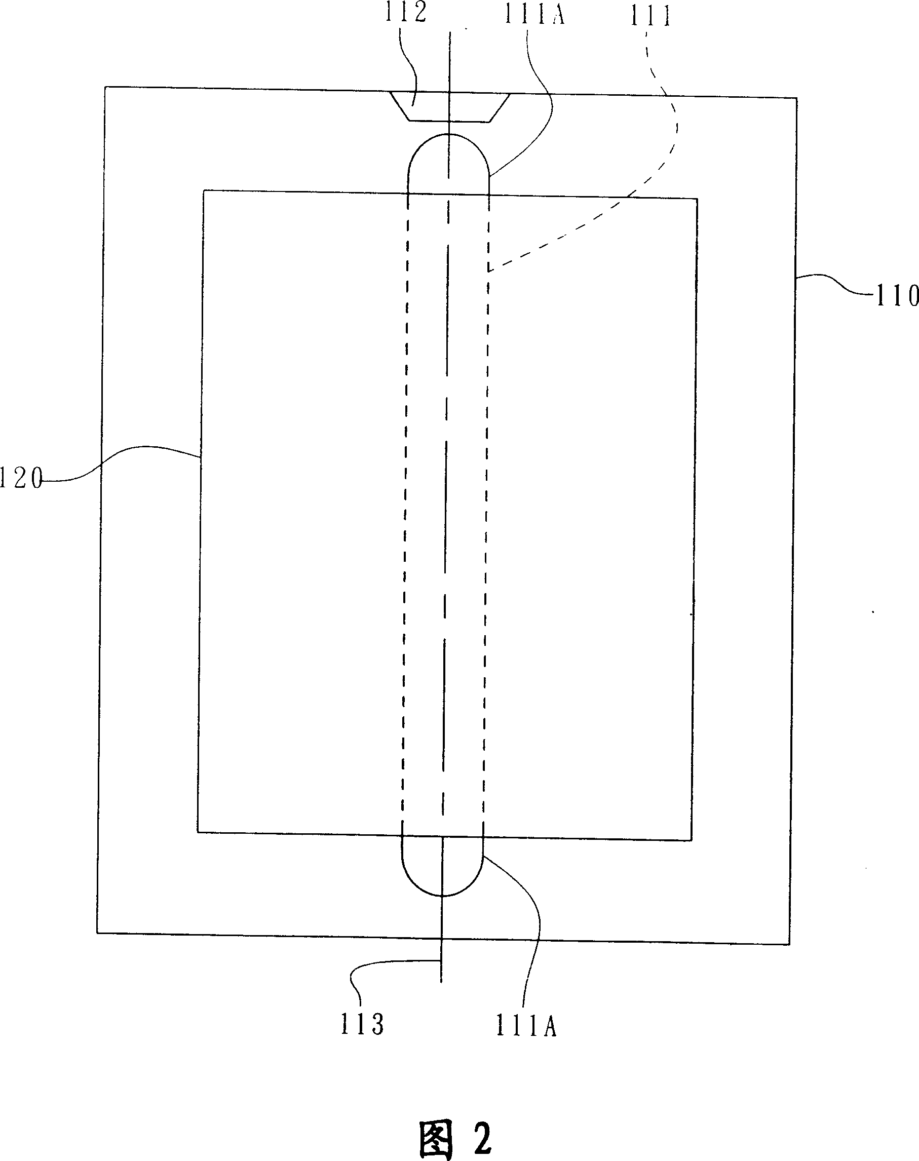
[0104] The substrate 210 is used as an IC carrier board and has circuit patterns for electrical transmis...


PUM

PropertyMeasurementUnit
Young's modulusaaaaaaaaaa

Abstract

The invention relates to the sealing structure for an integrated circuit and an anti-warping base plate of the structure. The sealing structure for the integrated circuit mainly comprises a base plate with a slot bore, a wafer, a covering colloid, at least one reinforcing colloid and a plurality of externally positioned terminals, the invention is characterized in that the young modulus of the reinforcing colloid is larger than that of the covering colloid while the curing shrinkage rate of the reinforcing colloid is smaller than that of the covering colloid, the covering colloid is formed on one surface of the base plate and at least covers part of the wafer while the reinforcing colloid protrudes from the other surface of the base plate and is connected with the external connection terminals on the same surface and is formed in the slot bore in order to touch with the wafer. Therefore, the reinforcing colloid is formed in a hidden place in the slot bore in order to increase the thickness of the reinforcing colloid and improve combination of the reinforcing colloid with the base plate, thus improving the anti-warping function of the sealing structure.

Description

technical field [0001] The invention relates to an integrated circuit packaging technology, in particular to an integrated circuit packaging structure capable of improving warpage resistance and its warpage-resistant substrate. Background technique [0002] In various traditional integrated circuit packaging technologies, there will be more or less warpage problems during the packaging process and when the surface of the packaged product is bonded. [0003] Please refer to FIG. 1 , which is a schematic cross-sectional view of a conventional integrated circuit package structure cut along the centerline of the minor axis. The integrated circuit package structure 100 of the window-type ball array package is based on a substrate 110 having a slot 111 to carry a chip 120 , and a die-bonding material 122 can be used to adhere the chip 120 . And by covering the chip 120 with an encapsulant 130 , a plurality of bonding wires 150 can be used to electrically connect the bonding pads ...

Claims


Application Information

Patent Timeline
IPC IPC(8): H01L23/28H01L23/50
CPCH01L2224/16225H01L2224/32225H01L2224/48091H01L2224/4824H01L2224/73204H01L2224/73215H01L2924/15311
Inventor 陈正斌范文正
Owner POWERTECH TECHNOLOGY
Why Eureka
Try Eureka