
EL key device and its making method

A technology of electroluminescence and manufacturing method, applied in electroluminescence light sources, electric light sources, lighting devices, etc., can solve the problems of uneven luminous brightness, uneven current distribution, poor circuit conduction, etc., and achieve uniform current distribution and cost. More, lower cost effect

Inactive Publication Date: 2008-02-13
TEEHWA TECH CORP
View PDF1 Cites 0 Cited by
  • Summary
  • Abstract
  • Description
  • Claims
  • Application Information

AI Technical Summary

Problems solved by technology

[0005] (1) Due to the conductive properties of the metal circuit layer 14 and the tin oxide layer 13, the distribution of the current is relatively uneven, and it is easier to have a larger current through the electroluminescent layer 15 near the metal circuit layer 14 and the electrode contact 19 , not only the current is less stable, but also the luminous brightness is less uniform
[0006] (2) During the manufacturing process of the existing electroluminescent device 10, it is often unavoidable to be affected by falling dust or other conductive particles
Due to the narrow line width of the metal circuit layer 14, if it is obstructed by falling dust, it will easily cause poor circuit conduction.
And if there are conductive particles attached, it is also easy to cause the subsequent formation of the electroluminescent layer 15 and the dielectric layer 16, the thickness at the position of the conductive particles is not uniform, or even the conductive particles directly contact the back conductive layer 17. short circuit
[0007] (3) The first and second cladding layers 12, 18 made of polyurethane (Polyurethane) film material are too soft and extensible in terms of structural characteristics, and are not suitable for use as those that require proper elasticity (recovery force). Structural features of the button device to use

Method used


Image

  • EL key device and its making method
  • EL key device and its making method
  • EL key device and its making method

Examples


Embodiment Construction

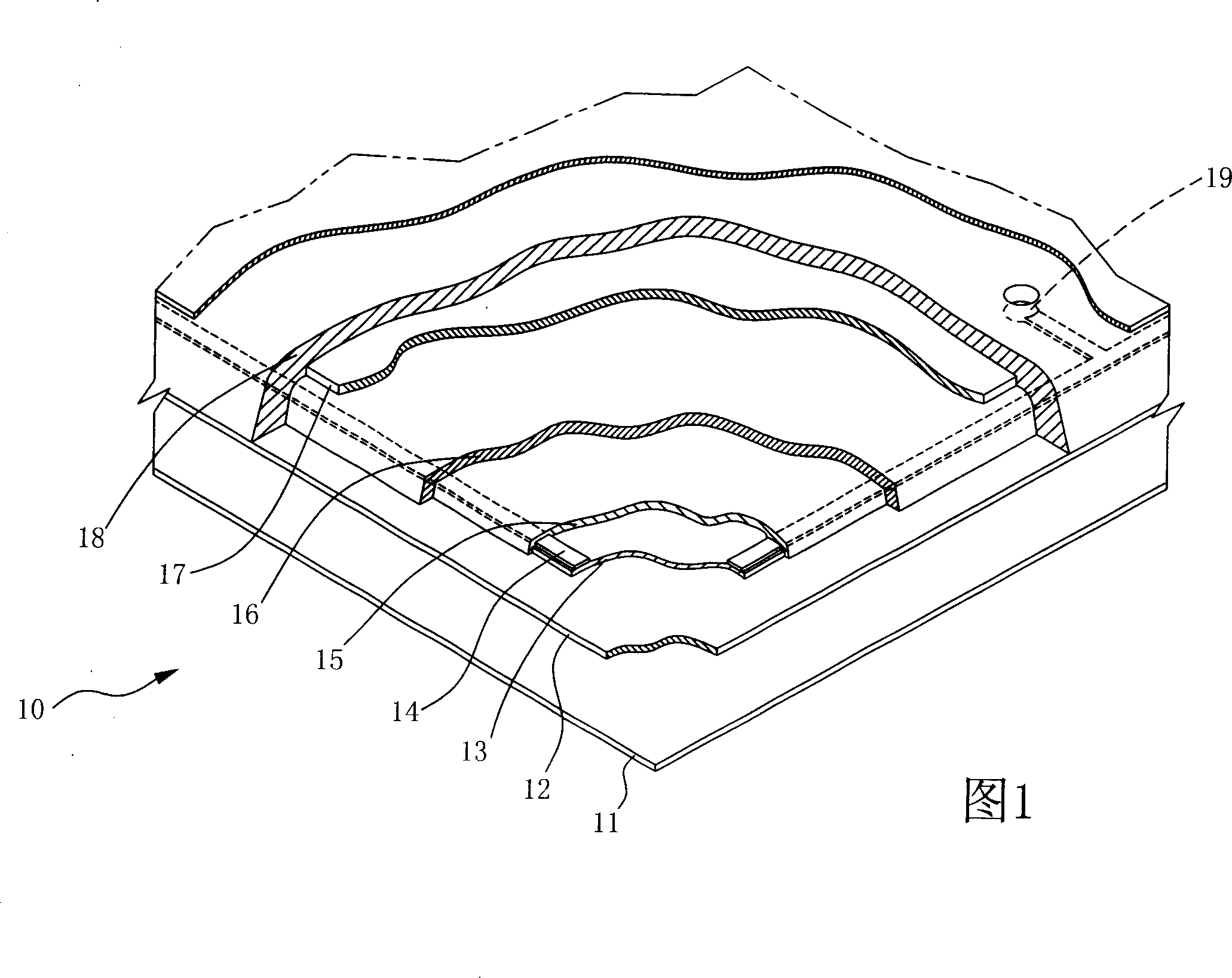
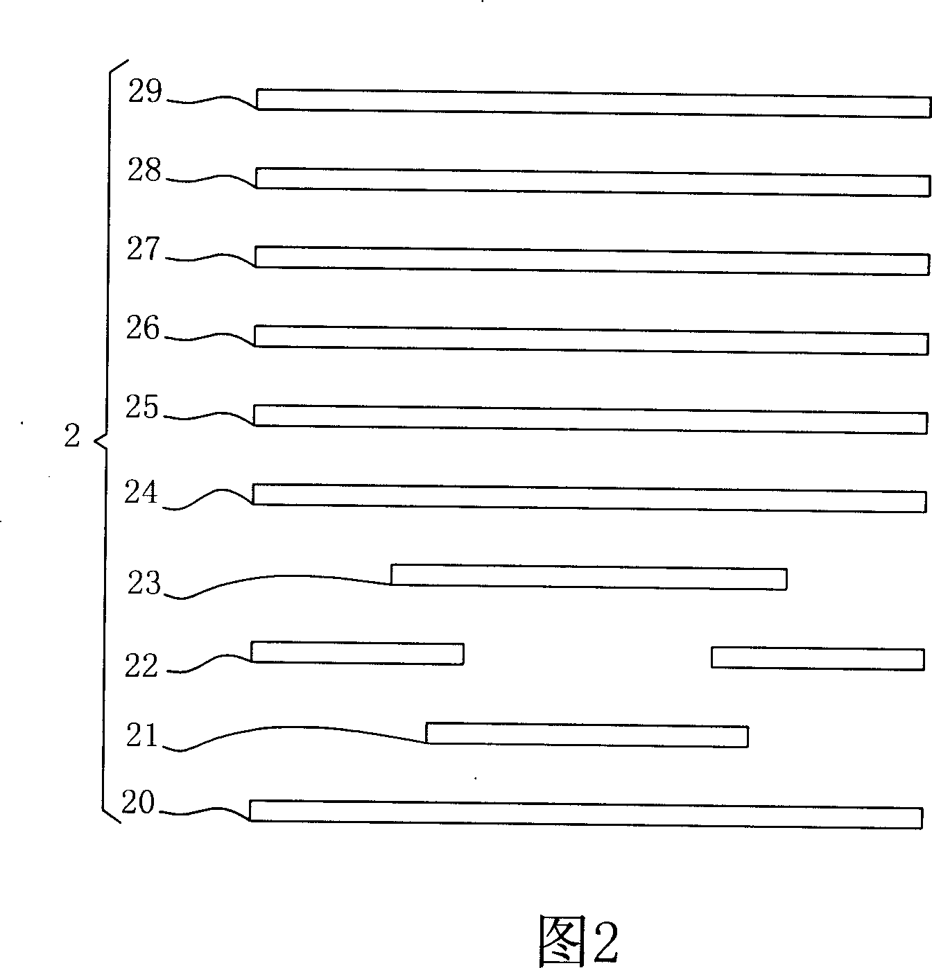
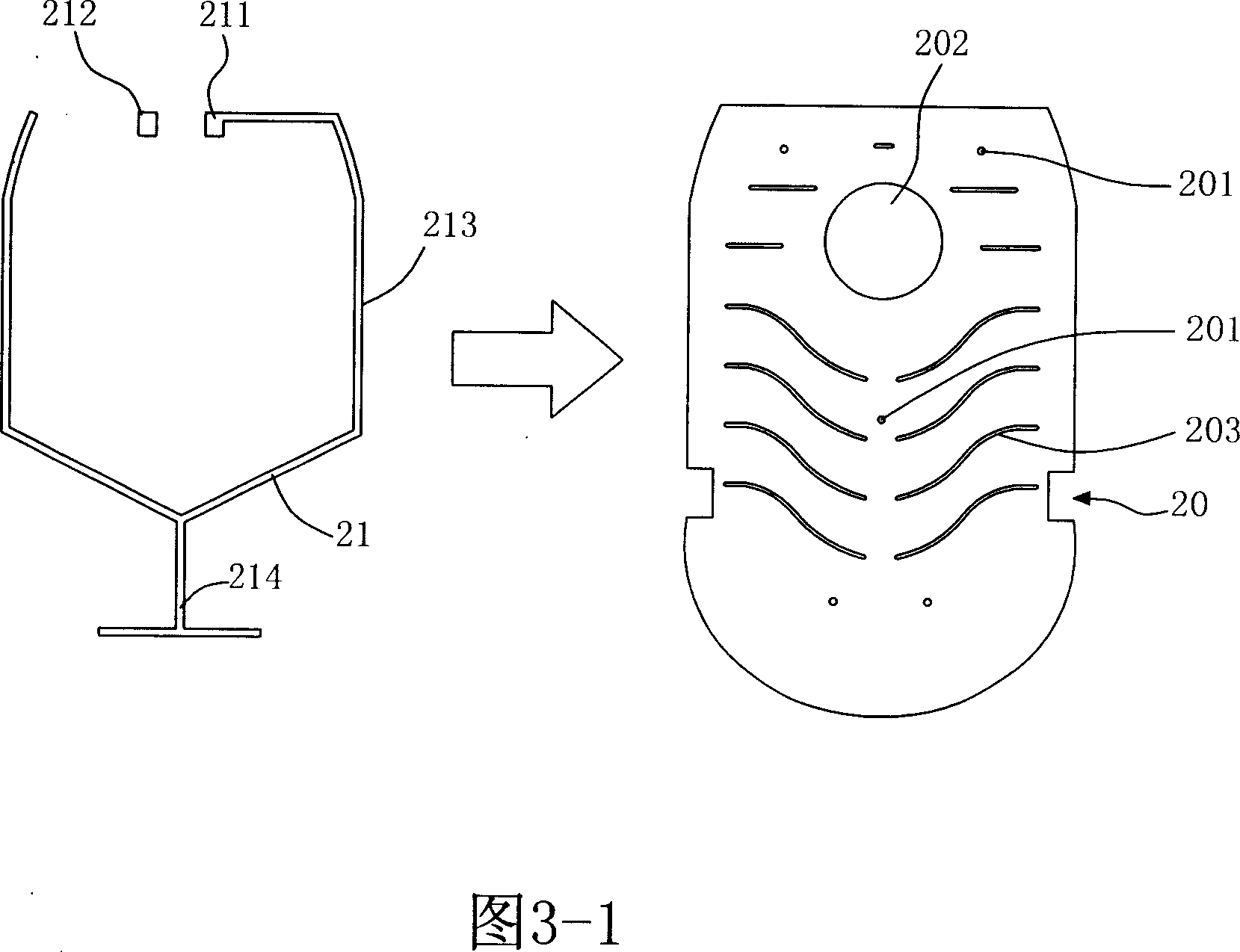
[0082] Please refer to FIG. 2 , FIG. 3-1 to FIG. 3-10 , and FIG. 4 , which disclose a preferred embodiment of the electroluminescence key device of the present invention. Wherein, FIG. 2 is a schematic diagram showing the composition sequence of each circuit layer in the electroluminescence key device of the present invention. 3-1 to 3-10 are schematic diagrams of the manufacturing process of the electroluminescence key device of the present invention. FIG. 4 is a three-dimensional exploded schematic diagram of each circuit layer of the electroluminescence key device of the present invention.

[0083] As shown in FIG. 2 and FIG. 4 , and referring to FIG. 3-1 to FIG. 3-10 , the manufacturing process of each circuit layer of the electroluminescence key device of the present invention is shown. The electroluminescence key device 2 of the present invention is mainly formed sequentially by printing on a substrate 20: a metal wire layer 21, a transparent insulating layer 22, a carb...


PUM


Abstract

The invention relates to an electroluminescent keystoke device and the manufacture method of the device. The invention mainly presses a metal wire layer, a transparency insulating layer, a carbon line layer, a transparent conducting layer, a luminous layer, a white dielectric layer, a carbon back layer, a silver back layer and a covering layer on a base plate of an electrically non-conductive material printed with keystoke letterforms in order. The settling of the carbon line layer and the carbon back layer can lead the applied current to be much uniformly arranged on the conducting layer and the silver back layer to avoid the phenomenon of uneven luminous brightness of partial areas in the luminous layer. And the setting of the transparency insulating layer can avoid bad circuit conduction caused by the factors of dust fall or adhered by other conducting impurities. Besides, the white dielectric layer can provide a capacity effect to reserve the instant electric power needed when the luminous layer is shining and can be a white background when the luminous layer is shining.

Description

technical field [0001] The present invention relates to an electroluminescent key device and its manufacturing method, especially a combination of an electroluminescent layer and related circuit layers on a key substrate. An electroluminescent key device that produces a soft cold light effect on the back of the key substrate. Background technique [0002] With the advancement of technology and the needs of consumers, many portable consumer electronic products have sprung up to be developed so that consumers can communicate, retrieve and use information at any time. In order to have more interaction with users, many portable consumer electronic products are equipped with keypads for users to input corresponding commands or characters. For example: smart phone (SmartPhone), personal digital assistant (Personal Digital Assistant; PDA), and notebook computer, etc. [0003] Someone in the industry once designed a mobile phone button device that can emit backlight, which not onl...

Claims


Application Information

Patent Timeline
IPC IPC(8): H05B33/00H05B33/10H05B33/12H01H9/00
Inventor 邓力升林诗岚
Owner TEEHWA TECH CORP
Learn More