
Forming method for protecting image

A technology for protecting graphics and graphics, applied in the field of forming protection graphics, can solve the problems of low degree of freedom of protection materials, less non-exposed parts, and reduced degrees of freedom, etc.

Active Publication Date: 2011-04-27
SANEI KAGAKU KK
View PDF1 Cites 0 Cited by
  • Summary
  • Abstract
  • Description
  • Claims
  • Application Information

AI Technical Summary

Problems solved by technology

[0007] However, solder resist materials are generally negative, and when direct exposure is performed, most of the patterned portion becomes the exposed portion, and the non-exposed portion is very small, so there is a concern that it will take a long time for direct exposure with laser light.
[0008] In addition, when the protective material is directly exposed to laser light, it is necessary to use a protective material with several times the sensitivity of the conventional one, so the protective material used is limited.
For example, when other components are mounted on a wiring board or a semiconductor substrate on which a protective film is patterned, the parts at the junction part on the wiring board need to have adhesiveness with resin or metal, but in this case, almost no A protective material that has both adhesion and sensitivity to laser light, but there is a concern that the degree of freedom in the selection of protective materials is low
As another example, when the protective film is made of a plating solution material, both chemical resistance and high sensitivity photosensitivity are required, and it is difficult to maintain chemical resistance and only increase the sensitivity
As a result, there is a concern that the degree of freedom in the choice of protective materials will decrease

Method used

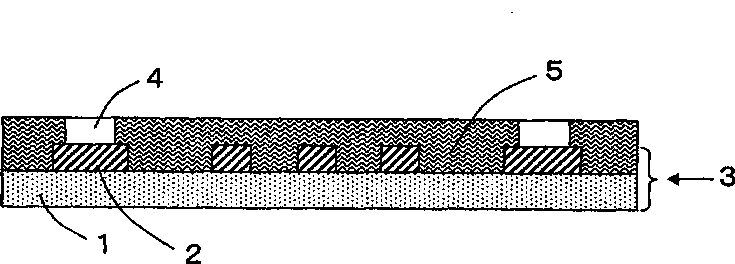
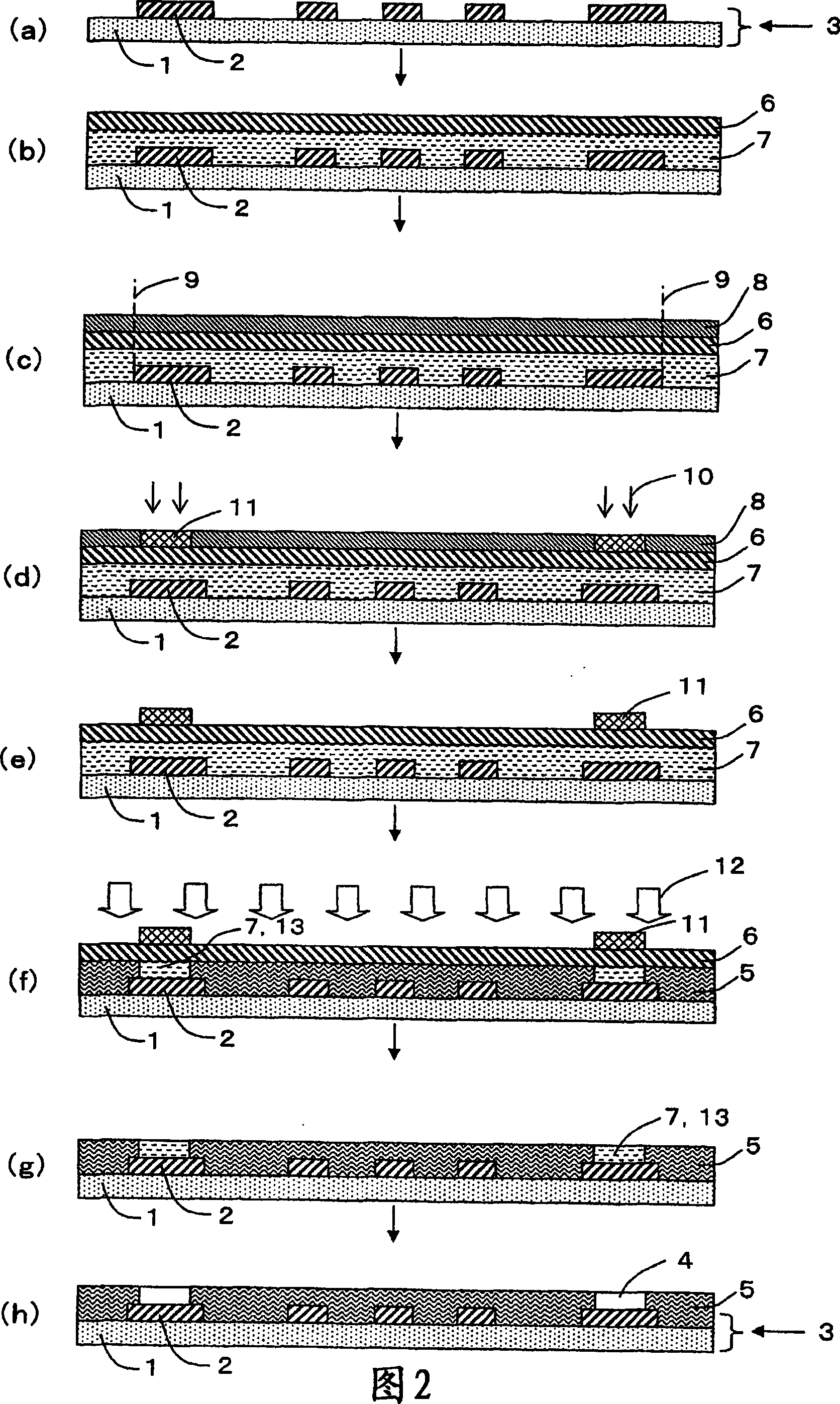
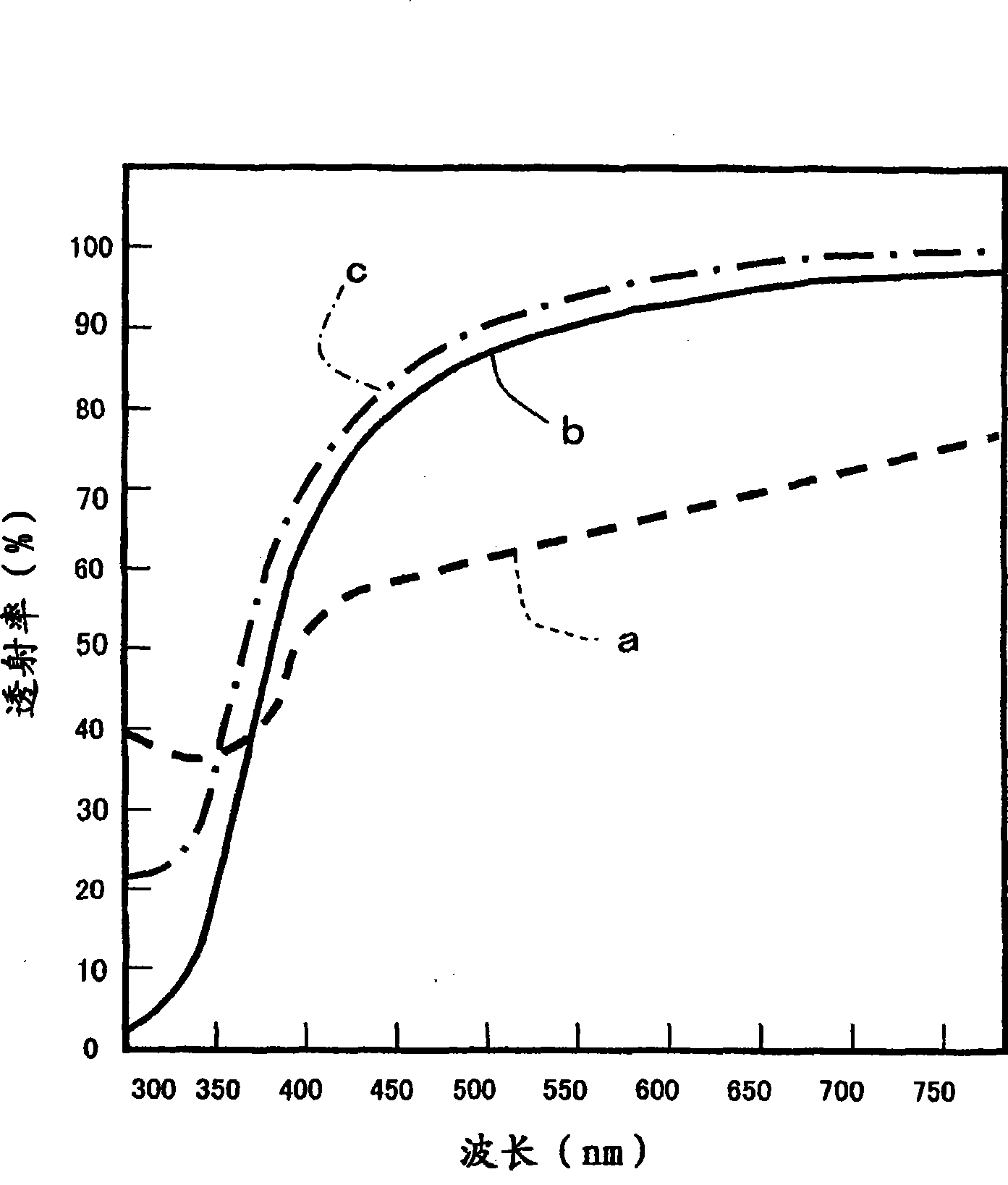

Image

  • Forming method for protecting image
  • Forming method for protecting image
  • Forming method for protecting image

Examples


Embodiment 1

[0161] First, use a 150-mesh polyester screen to uniformly disperse the following ingredients 1) The resin composition was printed on a PE film 14 with a thickness of 100 μm, and dried at 80° C. for 15 minutes. In this way, the second photocurable protective film 8 is formed on the PE film 14 . Thereafter, a PET masking film 6 having a thickness of 25 μm was laminated on the upper surface of the second photocurable protective film 8 . In this way, a 3-layer body consisting of the PE film 14, the second photocurable protective film 8 and the PET cover film 6 is made (refer to Figure 6 (a)).

[0162] On the other hand, the following combination composition 2) Alkali developing type solder resist is screen-printed on the printed wiring board 3 on which the wiring pattern 2 has been formed, and the first photocurable protective film 7 is formed on the printed wiring board 3 (refer to Figure 6 (b)).

[0163] Next, the above-mentioned three-layer body was laminated on the fir...


PUM

PropertyMeasurementUnit
particle sizeaaaaaaaaaa
acid valueaaaaaaaaaa
particle sizeaaaaaaaaaa

Abstract

The invention provides a resist pattern forming method which can perform exposure of solder material and perform exposure using laser light by the same solder material. A solder film 7 with UV photosensitivity covered by cover film 6 is formed on the print wiring board 3 and a protective film 8 with visible photosensitivity for screening UV is formed above the solder film 7. The visible light laser 10 is used to expose. A resist pattern 11 is exposed on the protective film 8 and the water is used to develop to form solidifying film of protective film 8, and a mask parttern is generated by theresist pattern 11. Subsequently, using UV, the said mask parttern is used as mask and a solder film 5 is exposed on the solder film 7. A weak base developing liquid is used to develop. A solder pattern 5 generated by solidifying film of solder film 7 is formed on the print wiring board 3.

Description

[0001] technology area [0002] The present invention relates to a method for forming a resist pattern, and in particular to a resist pattern that can shorten exposure time and improve production efficiency when forming a pre-set solder resist when soldering on a printed wiring board. A formation method, and a formation method of a protective pattern that can increase the degree of freedom used in solder resist. Background technique [0003] In the manufacture of printed wiring boards, photosensitive materials are used as etching resist materials for circuit formation or solder resist materials for circuit protection. [0004] Conventionally, when pattern-exposing these protective materials, it is common to develop a construction method by irradiating ultraviolet light through a mask (hereinafter also referred to as a mask) formed with a light-shielding negative pattern such as glass or film. [0005] However, in the case of pattern exposure using a mask, it takes cost and ti...

Claims


Application Information

Patent Timeline
Patent Type & Authority Patents(China)
IPC IPC(8): G03F1/14G03F7/20G03F7/00H05K3/06G03F7/004G03F7/027G03F7/26G03F7/32H05K3/18H05K3/28
CPCH05K3/0082H05K2203/0551H05K2203/107H05K3/28G03F7/095H05K2203/066H05K2203/0577G03F7/038G03F7/0045G03F7/0047G03F7/0382H01L21/027H01L21/0271
Inventor 北村和宪佐藤清井上荣一
Owner SANEI KAGAKU KK
Learn More