

CMOS device manufacturing method having different lateral wall bulkhead width
A device manufacturing method and sidewall spacing technology, applied in semiconductor/solid-state device manufacturing, electrical components, circuits, etc., can solve threshold voltage, drive current and saturation leakage current differences, CMOS device performance symmetry and consistency degradation, etc. problem, the effect of reaching threshold voltage and saturation leakage current improvement
- Summary
- Abstract
- Description
- Claims
- Application Information
AI Technical Summary
Problems solved by technology
Method used
Image

Examples
Embodiment Construction
[0014] In order to make the above objects, features and advantages of the present invention more comprehensible, specific implementations of the present invention will be described in detail below in conjunction with the accompanying drawings.
[0015] In the following description, numerous specific details are set forth in order to provide a thorough understanding of the present invention. However, the present invention can be implemented in many ways other than those described here, and those skilled in the art can make similar extensions without departing from the connotation of the present invention. Accordingly, the invention is not limited to the specific implementations disclosed below.
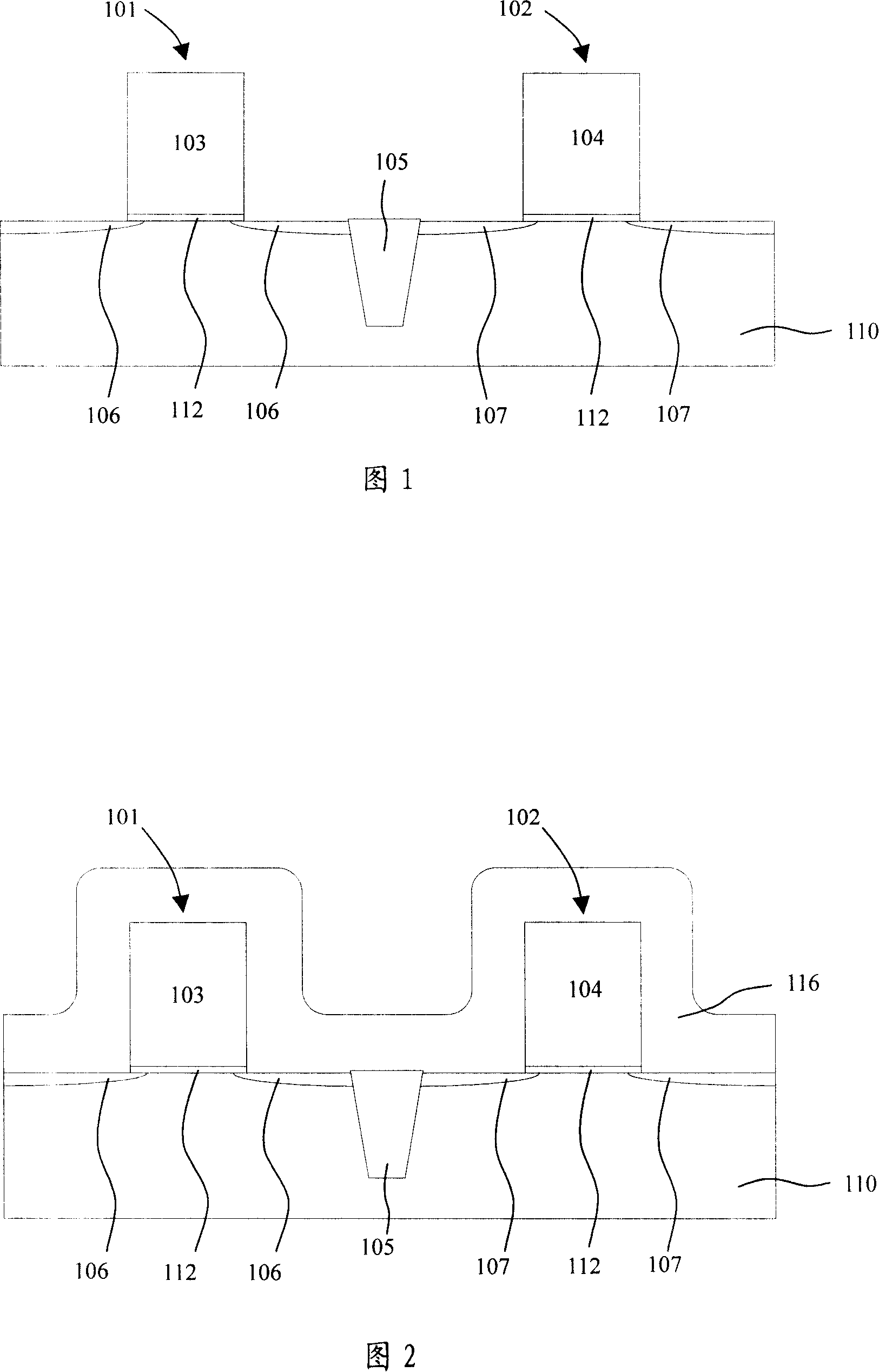
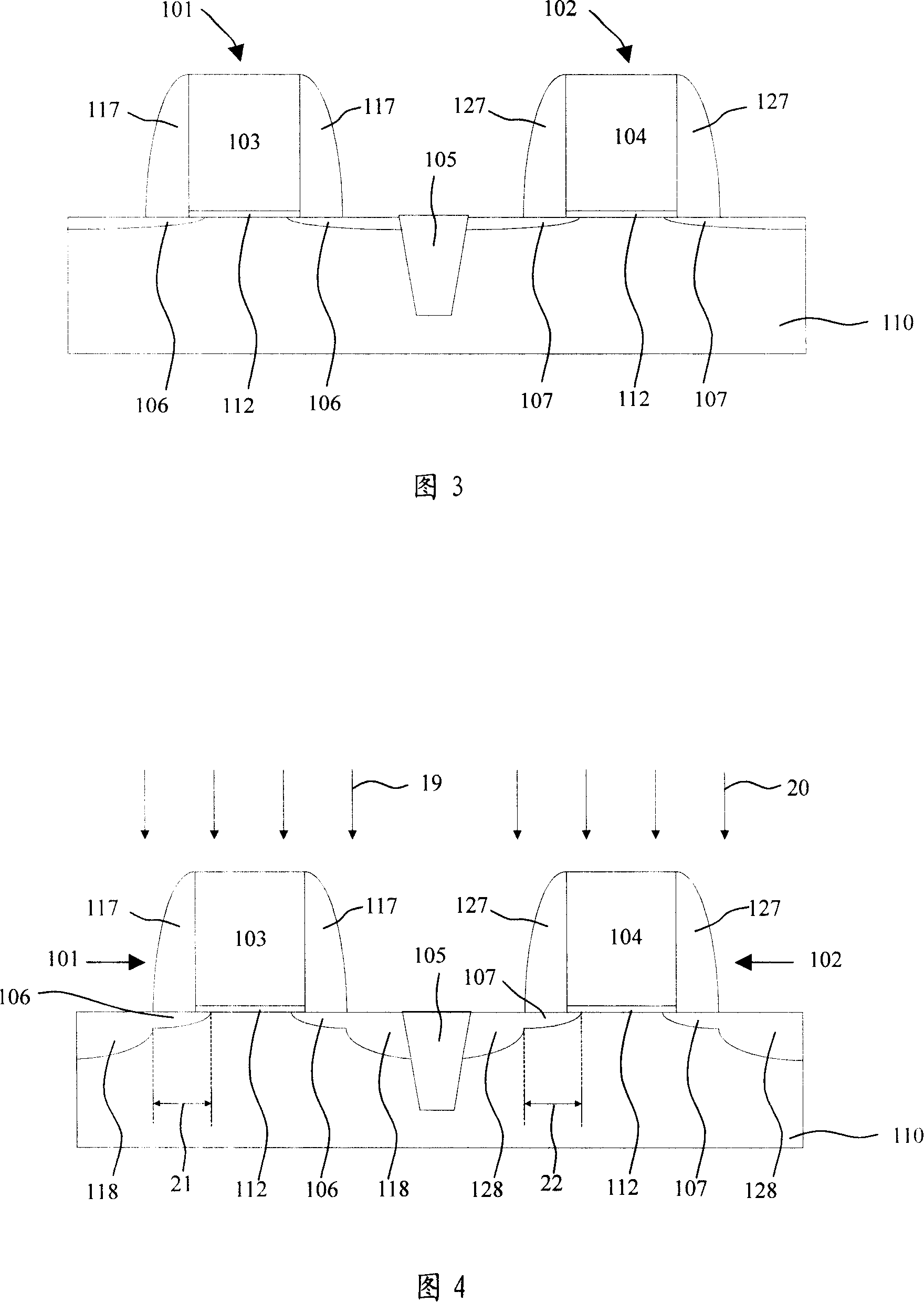
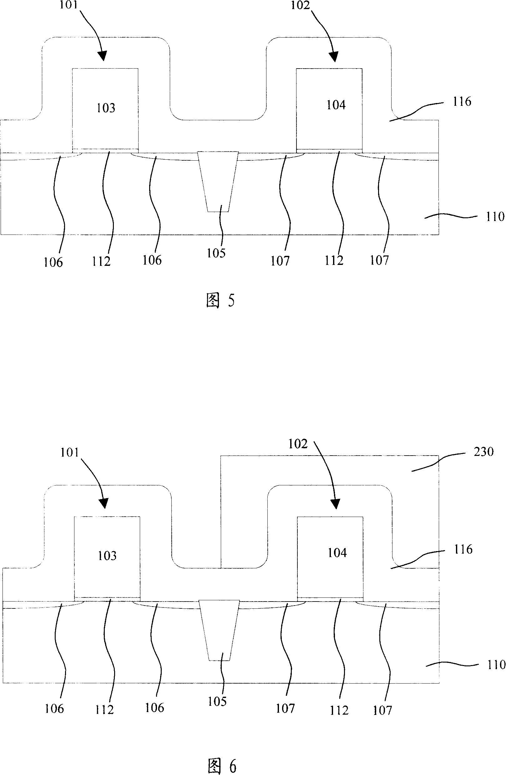
[0016] In CMOS devices, the n-channel of NMOS and the p-channel of PMOS are formed on the same substrate, and the length of the channel is determined by the width of the sidewall spacer. The respective conduction characteristics of NMOS and PMOS transistors are obtained by performing ...
PUM
 Abstract
Description
Claims
Application Information