X-ray detector with in-pixel processing circuits

A technology of X-ray and detector, which is applied in the field of medical imaging equipment and the manufacture of this kind of X-ray detector, can solve the problems of damage and processing circuit X-ray interference, etc.

Inactive Publication Date: 2008-03-12
KONINKLIJKE PHILIPS ELECTRONICS NV
View PDF3 Cites 34 Cited by
  • Summary
  • Abstract
  • Description
  • Claims
  • Application Information

AI Technical Summary

Problems solved by technology

A problem with this approach, however, is that the processing circuitry often includes components that are susceptible to, or even destroyed by, X-rays

Method used


Image

  • X-ray detector with in-pixel processing circuits
  • X-ray detector with in-pixel processing circuits

Examples


Embodiment Construction

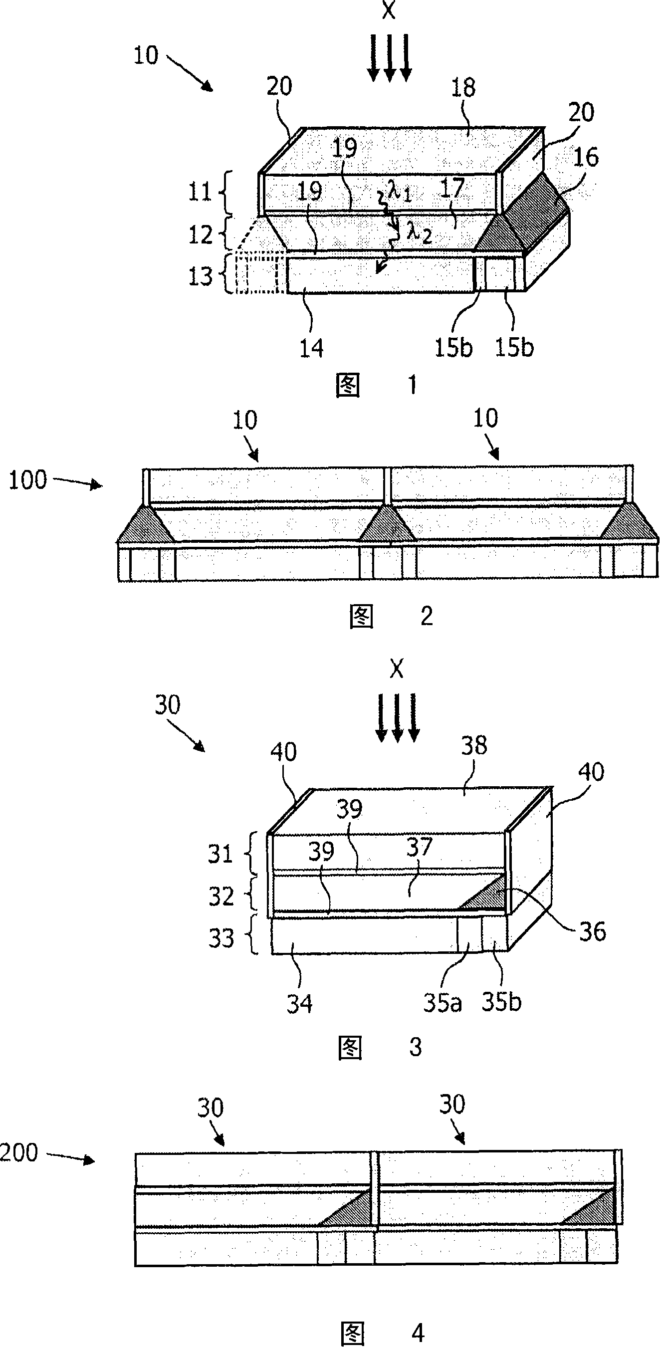
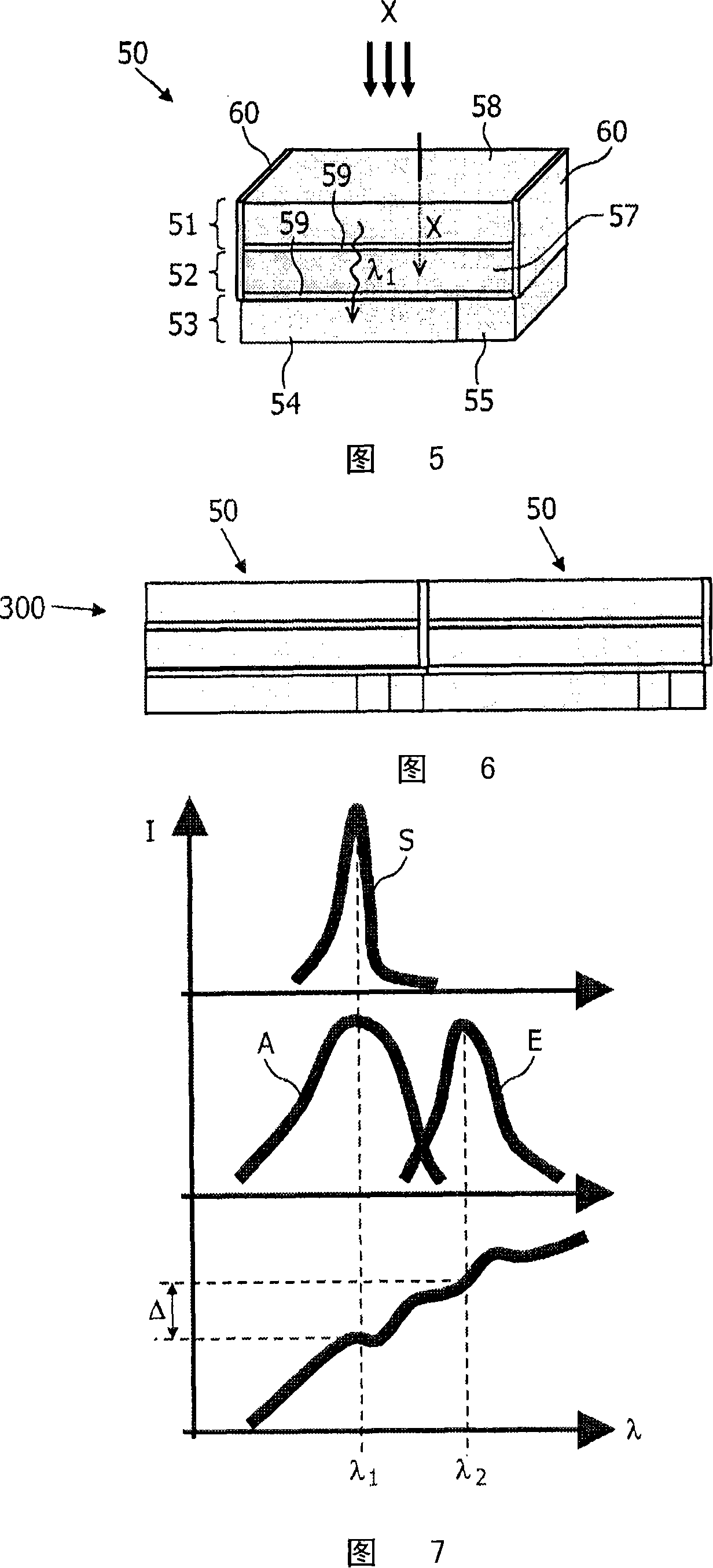
[0033]In prior art computed tomography (CT), scintillator pixel elements placed on Si photodiodes or on top of both CMOS photodiodes and integrated radiation-sensitive in-pixel electronics are used as X-ray detectors. Electronics are now protected from X-rays by lead spacers between adjacent scintillator elements. This technique is expensive to manufacture, construct and set up, and has the disadvantage of resulting in a sub-optimal DQE (Detection Quantum Efficiency). An alternative method of shielding the electronics is to employ the scintillator material itself. Since it must be thick enough to adequately absorb X-rays, it can adversely affect light output and efficiency due to reduced light transmission (also, thicker layers are also more expensive). If the thickness of the scintillator material is not sufficient for adequate shielding, a certain amount of X-ray radiation will pass through this material without any reaction and thus cause radiation damage to photodiodes, e...


PUM


Abstract

The invention relates to an X-ray detector with an array of pixels (10) that are composed of a scintillation layer (11), a coupling layer (12), and a sensitive layer (13). The coupling layer (12) comprises light guiding units (17) and shielding units (16), wherein the shielding units (16) are disposed above electronic processing circuits (15a, 15b) that are susceptible to disturbances by X-radiation. In an alternative embodiment, the coupling layer comprises a material like lead-glass that is transparent for light and absorbing for X-radiation. Preferably a wavelength- shifting material incorporated into the coupling layer (12) shifts the wavelength (1) of the photons generated in the scintillation layer (11) to values 2) at which the sensitive layer (13) has a higher sensitivity.

Description

technical field [0001] The invention relates to an X-ray detector having a sensitive layer of a detector element (pixel) comprising a processing circuit susceptible to X-ray interference. In addition, it includes a method of manufacturing such an X-ray detector. The invention also relates to a medical imaging device having such a detector. Background technique [0002] X-ray detectors with sensitive layers or arrays of sensor elements are used, for example, in computed tomography (CT) scanners. In so-called "indirect conversion" X-ray detectors, a scintillation layer is placed above the sensitive layer to convert incident X-rays into visible light photons, which are then converted into electrical signals by sensor cells in the sensitive layer. In many modern detectors, post-processing (amplification, filtering, etc.) of the electrical signal is largely done by "in-pixel" processing circuitry, ie electronic circuitry integrated directly into each detector element (pixel). ...

Claims


Application Information

Patent Timeline
Patent Type & Authority Applications(China)
IPC IPC(8): G01T1/202
CPCG01T1/202
Inventor G·泽特勒G·沃格特-迈耶
Owner KONINKLIJKE PHILIPS ELECTRONICS NV
Why Eureka
Try Eureka