Semiconductor device and its production method
A gate and silicon substrate technology, applied in the field of semiconductor devices and their manufacturing, can solve the problems of increased short channel effect, reduced effective length of gate channel, serious hot carrier effect overlapping capacitance, etc.
- Summary
- Abstract
- Description
- Claims
- Application Information
AI Technical Summary
Problems solved by technology
Method used
Image

Examples
Embodiment Construction
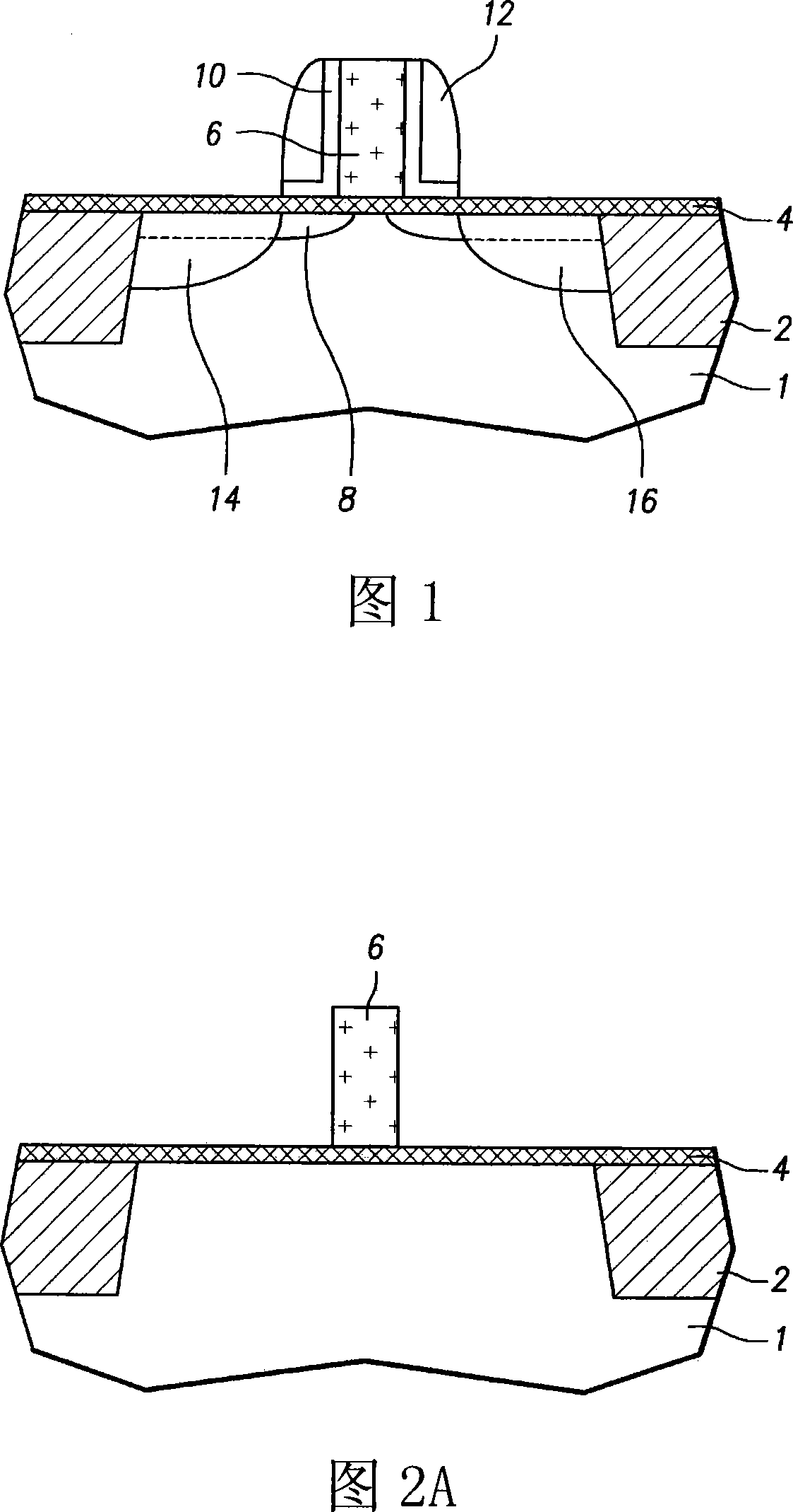
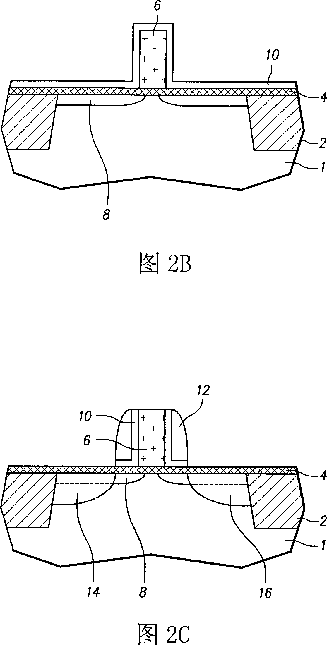
[0032] As shown in the example of FIG. 4 , described in accordance with an embodiment is a semiconductor device that includes a device isolation layer 102 that may be formed on and / or over a silicon substrate. The device isolation layer 102 can divide the silicon substrate 101 into an active area and an inactive area. Gate 106 may be formed on and / or over silicon substrate 101 . A gate oxide layer 108 is formed around the sidewalls of the gate 106 to a height that exposes the upper portion of the gate 106 . A gate insulating layer 104 may be interposed between the silicon substrate 101 and the gate electrode 106 . An epitaxial layer 110 having a width greater than that of the gate 106 and the gate insulating layer 104 may be formed on and / or over the gate 106 , especially on and / or over the active region of the gate 106 . The epitaxial layer 110 may be formed to have a mushroom-like shape. LDD regions 112 may be formed in the surface of the silicon substrate 101 around the ...
PUM
 Abstract
Description
Claims
Application Information
 - R&D
- Intellectual Property
- Life Sciences
- Materials
- Tech Scout
- Unparalleled Data Quality
- Higher Quality Content
- 60% Fewer Hallucinations
Browse by: Latest US Patents, China's latest patents, Technical Efficacy Thesaurus, Application Domain, Technology Topic, Popular Technical Reports.
© 2025 PatSnap. All rights reserved.Legal|Privacy policy|Modern Slavery Act Transparency Statement|Sitemap|About US| Contact US: help@patsnap.com