Discharge type display device
A technology for display devices and discharge spaces, applied in discharge tubes, AC plasma display panels, electrode configurations, etc., can solve problems such as poor luminous efficiency and low brightness of display devices, and achieve the effect of preventing color deviation and suppressing deterioration
- Summary
- Abstract
- Description
- Claims
- Application Information
AI Technical Summary
Problems solved by technology
Method used
Image
Examples
Embodiment approach 1
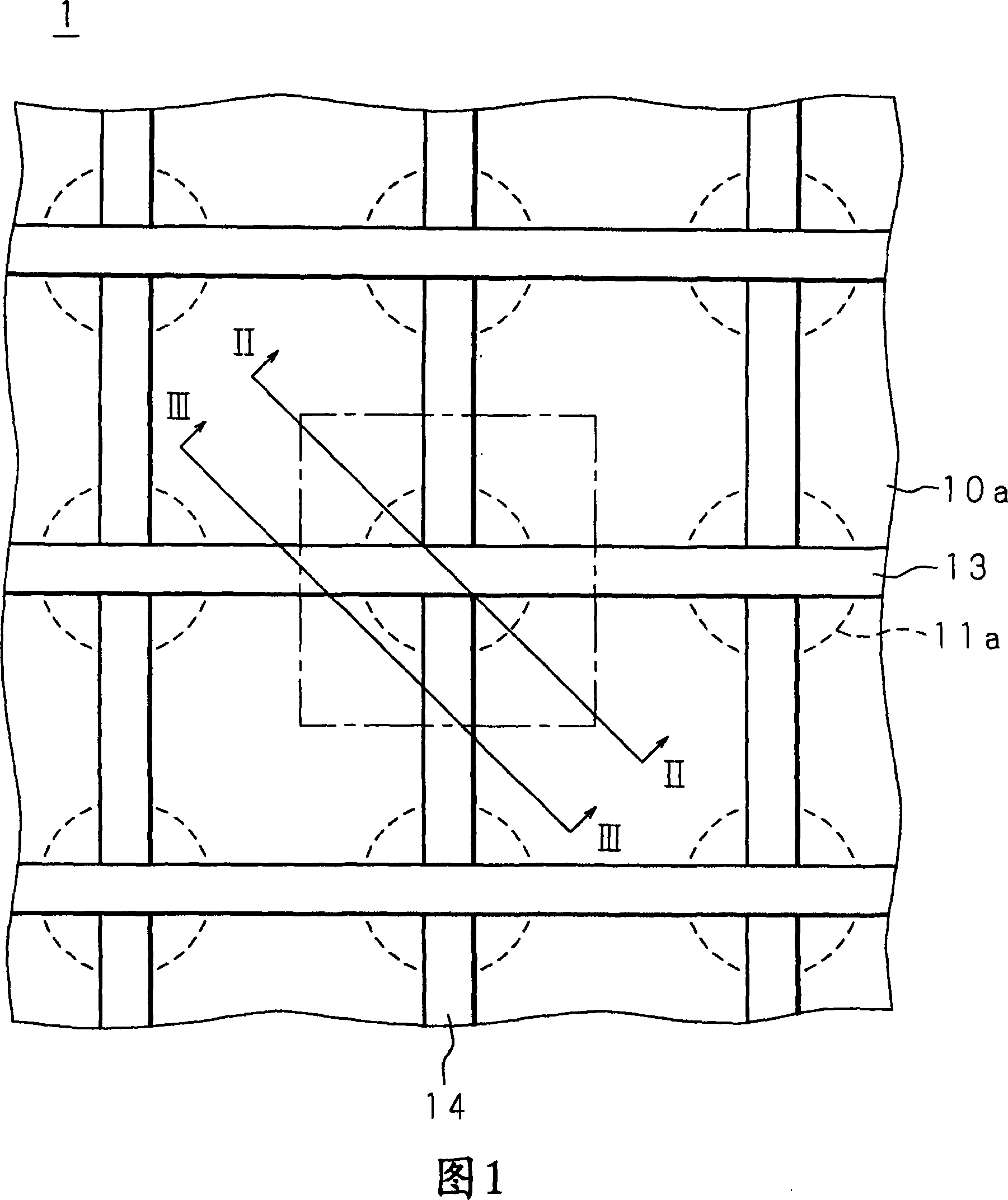
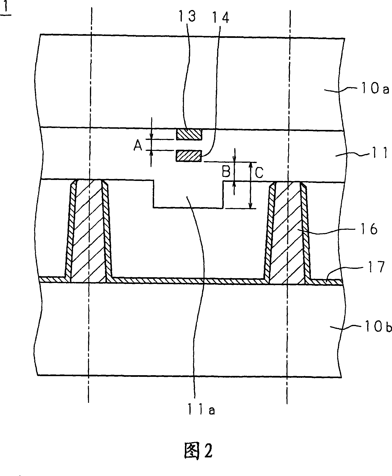
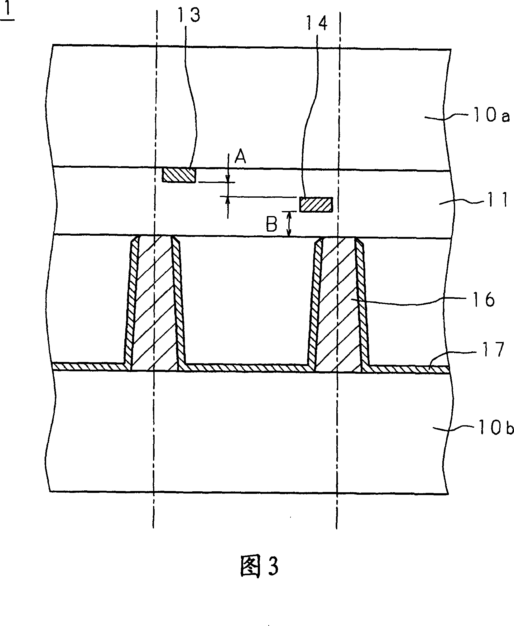
[0059] FIG. 1 is a schematic plan view of a discharge display device according to Embodiment 1 of the present invention. Fig. 2 is a structural sectional view along line II-II of Fig. 1 . Fig. 3 is a sectional view of the structure along line III-III of Fig. 1 .
[0060] Discharge display device 1 according to Embodiment 1 of the present invention has a structure in which front substrate 10a and rear substrate 10b, such as a glass plate having excellent transmittance in the visible light region, are arranged to face each other, and low-melting-point glass is used for passage. A discharge medium such as Xe—Ne, Xe—He is sealed in the space (discharge space) created by sealing the peripheral portions of the facing surfaces of front substrate 10a and rear substrate 10b with a sealing material such as paste.
[0061] A dielectric layer 11 for accumulating wall charges is formed on the front substrate 10a, and first electrodes 13 and second electrodes 14 perpendicular to each other...
Embodiment approach 2
[0072] In Embodiment 1, a discharge type display device is described in which the first electrode and the second electrode for inducing sustain discharge are provided on one substrate (front substrate), but the first electrode and the second electrode are not necessarily required. The example in which they are provided on the same substrate is described in Embodiment Mode 2. 8 and 9 are sectional views of the structure of the discharge display device according to Embodiment 2 of the present invention, and the plan views are omitted because they are the same as those in FIG. 1 . 8 corresponds to a cross-sectional view of the structure along line II-II in FIG. 1 , and FIG. 9 corresponds to a cross-sectional view of the structure along line III-III in FIG. 1 .
[0073] A dielectric layer 21 for accumulating wall charges is formed on the front substrate 10a, and first electrodes 23 are formed inside the dielectric layer 21 at a predetermined pitch. On the other hand, a dielectric...
Embodiment approach 3
[0076] In Embodiment 2, the discharge type display device in which the dielectric layer on the front substrate side is thicker on the discharge space side than the other regions is described, but the dielectric layer on the back substrate side may be thicker on the discharge space side. The case where one side is thicker than the other regions is described in Embodiment 3. 10 is a cross-sectional view showing the structure of a discharge display device according to Embodiment 3 of the present invention, and its plan view is omitted because it is the same as FIG. 1 . Furthermore, FIG. 10 corresponds to a structural sectional view taken along line II-II in FIG. 1 .
[0077] A dielectric layer 31 for accumulating wall charges is formed on the front substrate 10a, and first electrodes 33 are formed inside the dielectric layer 31 at a predetermined pitch. On the other hand, a dielectric layer 32 is formed on the rear substrate 10b, and second electrodes 34 perpendicular to the fir...
PUM
 Abstract
Description
Claims
Application Information


