Supercharge Your Innovation With Domain-Expert AI Agents!

Tri-states one-time programmable memory (otp) cell

A memory component and memory technology, applied in static memory, read-only memory, electrical components, etc., to achieve the effect of novel circuit and low cost

Active Publication Date: 2008-04-02
重庆万国半导体科技有限公司
View PDF3 Cites 0 Cited by
  • Summary
  • Abstract
  • Description
  • Claims
  • Application Information

AI Technical Summary

Problems solved by technology

Accordingly, there remains a need in the art to provide improved memory configurations and methods of manufacturing, applying standard foundry processes, and three-state provision of OTP memory elements that allow storage and readout of data bit storage in OTP memory, so that currently in the prior art The above-mentioned difficulties encountered can be resolved

Method used


Image

  • Tri-states one-time programmable memory (otp) cell
  • Tri-states one-time programmable memory (otp) cell
  • Tri-states one-time programmable memory (otp) cell

Examples


Embodiment Construction

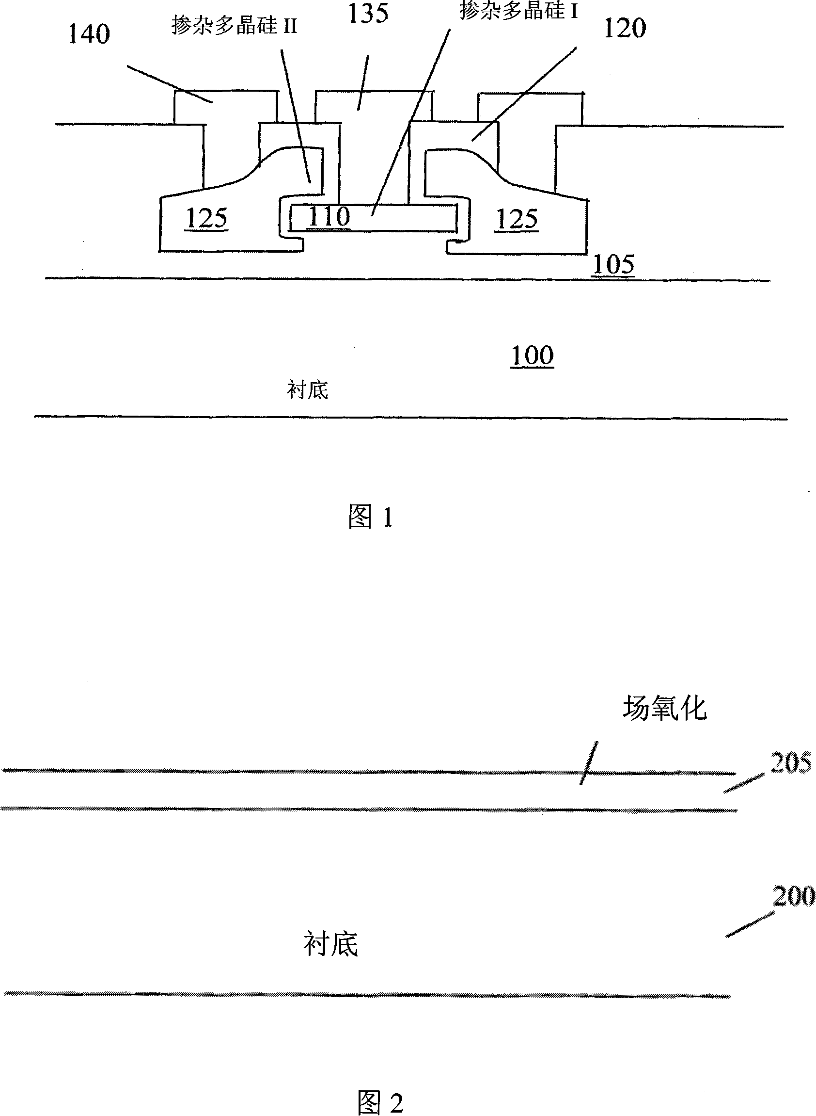
[0019]Referring to FIG. 1 , the OTP memory element of the present invention is supported on a thick field oxide layer 105 formed on the top surface of a semiconductor substrate 100 . This thick field oxide layer 105 insulates the components from the substrate 100 . The first doped polysilicon region 110 is invaded from the second doped polysilicon region 125 with a thin layer of low voltage gate oxide 120 . Each polysilicon region has electrodes such as electrodes 135 and 140 respectively connected for data recording and reading. The thin gate oxide layer 120 between the two doped polysilicon regions prevents conduction between the two doped polysilicon regions 110 and 125 . However, the conduction state between the two doped polysilicon regions 110 and 125 can be changed for memory programming purposes. In the process of programming a memory element as shown in FIG. 1 , a high voltage may be applied to the electrodes between doped polysilicon regions 110 and 125 . When the...


PUM


Abstract

A method of performing a programming, testing and trimming operation is disclosed in this invention. The method includes a step of applying a programming circuit for programming an OTP memory for probing and sensing one of three different states of the OTP memory for carrying out a trimming operation using one of the three states of the OTP memory whereby a higher utilization of OTP memory cells is achieved. Selecting and programming two conductive circuits of the OTP into two different operational characteristics thus enables the storing and sensing one of the three different states of the OTP memory. These two conductive circuits may include two different transistors for programming into a linear resistor and a nonlinear resistor with different current conducting characteristics. The programming processes include application of a high voltage and different programming currents thus generating different operational characteristics of these two transistors.

Description

technical field [0001] The present invention generally relates to the structure and manufacturing process of a programmable memory device, and the circuit configuration and operation method of the programmable memory device. More particularly, the present invention relates to improved device configurations and novel circuit configurations and methods of operation for implementing three-state one-time programmable memory elements. Background technique [0002] In order to reduce the production cost and shorten the time-to-market cycle of integrated circuit products, design departments are increasingly relying on readily available foundry processes for their prototyping and manufacturing. However, adjusting the device features designed for back-end packaging requires additional Intellectual Property (IP, Intellectual Property) modules or fuzes. These IP blocks can include One Time Programmable (OTP, One Time Program) memory or Electrically Erasable Programmable Read Only Memo...

Claims


Application Information

Patent Timeline
Patent Type & Authority Applications(China)
IPC IPC(8): G11C17/16H01L27/115H10B69/00
Inventor 胡永中张育诚戴嵩山
Owner 重庆万国半导体科技有限公司
Features
  • R&D
  • Intellectual Property
  • Life Sciences
  • Materials
  • Tech Scout
  • Unparalleled Data Quality
  • Higher Quality Content
  • 60% Fewer Hallucinations
Learn More