Semiconductor technology processing system and processing method thereof

A technology for semiconductors and process parts, which is applied in the field of semiconductor process processing systems and its processing, and can solve the problems of low reliability and complex mechanical structures of mass production devices for process parts

Active Publication Date: 2008-05-07
ADVANCED MICRO FAB EQUIP INC CHINA
View PDF2 Cites 19 Cited by
  • Summary
  • Abstract
  • Description
  • Claims
  • Application Information

AI Technical Summary

Problems solved by technology

[0012] The purpose of the present invention is to provide a semiconductor process processing system that solves the

Method used


Image

  • Semiconductor technology processing system and processing method thereof
  • Semiconductor technology processing system and processing method thereof
  • Semiconductor technology processing system and processing method thereof

Examples


Embodiment Construction

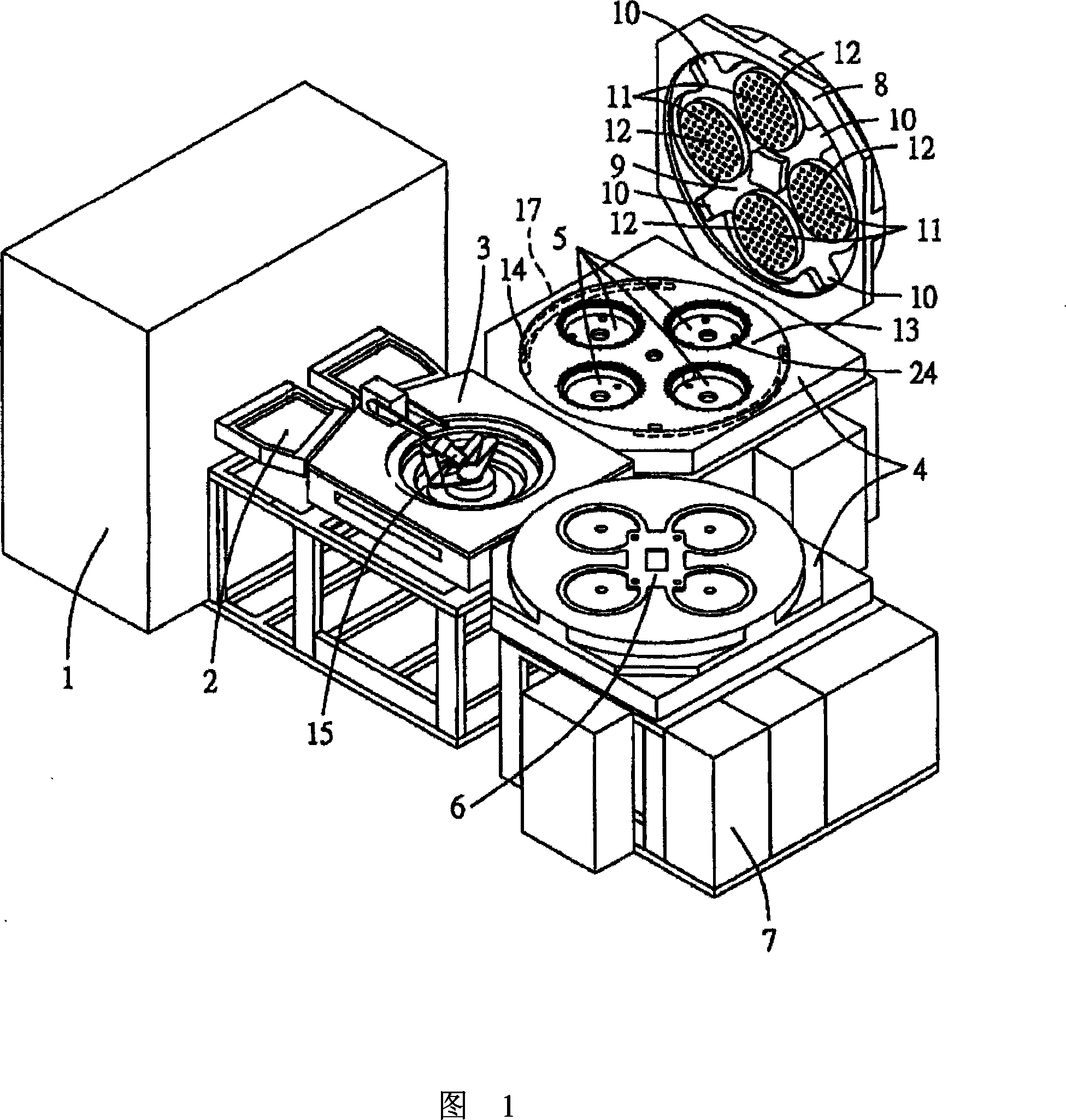
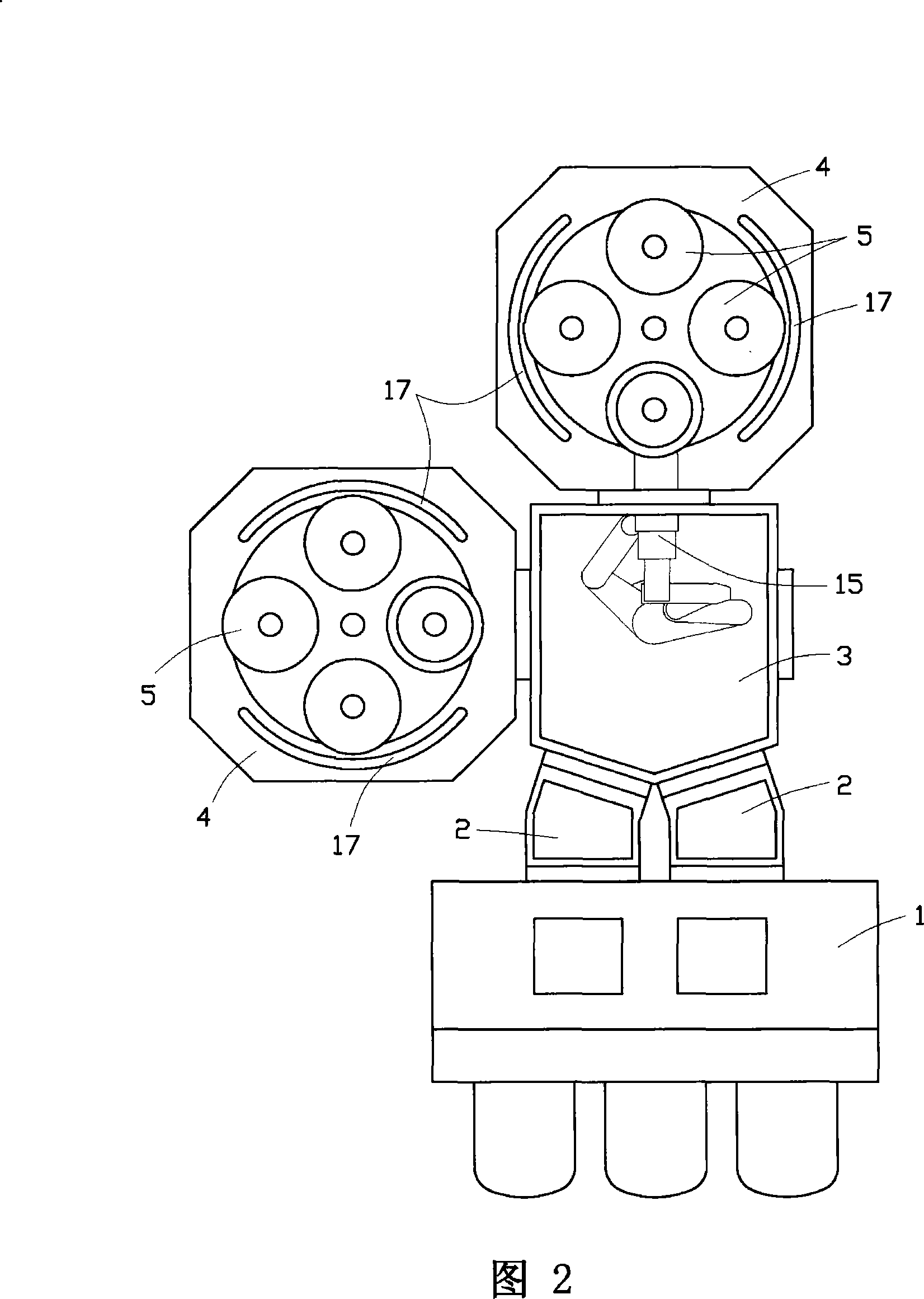
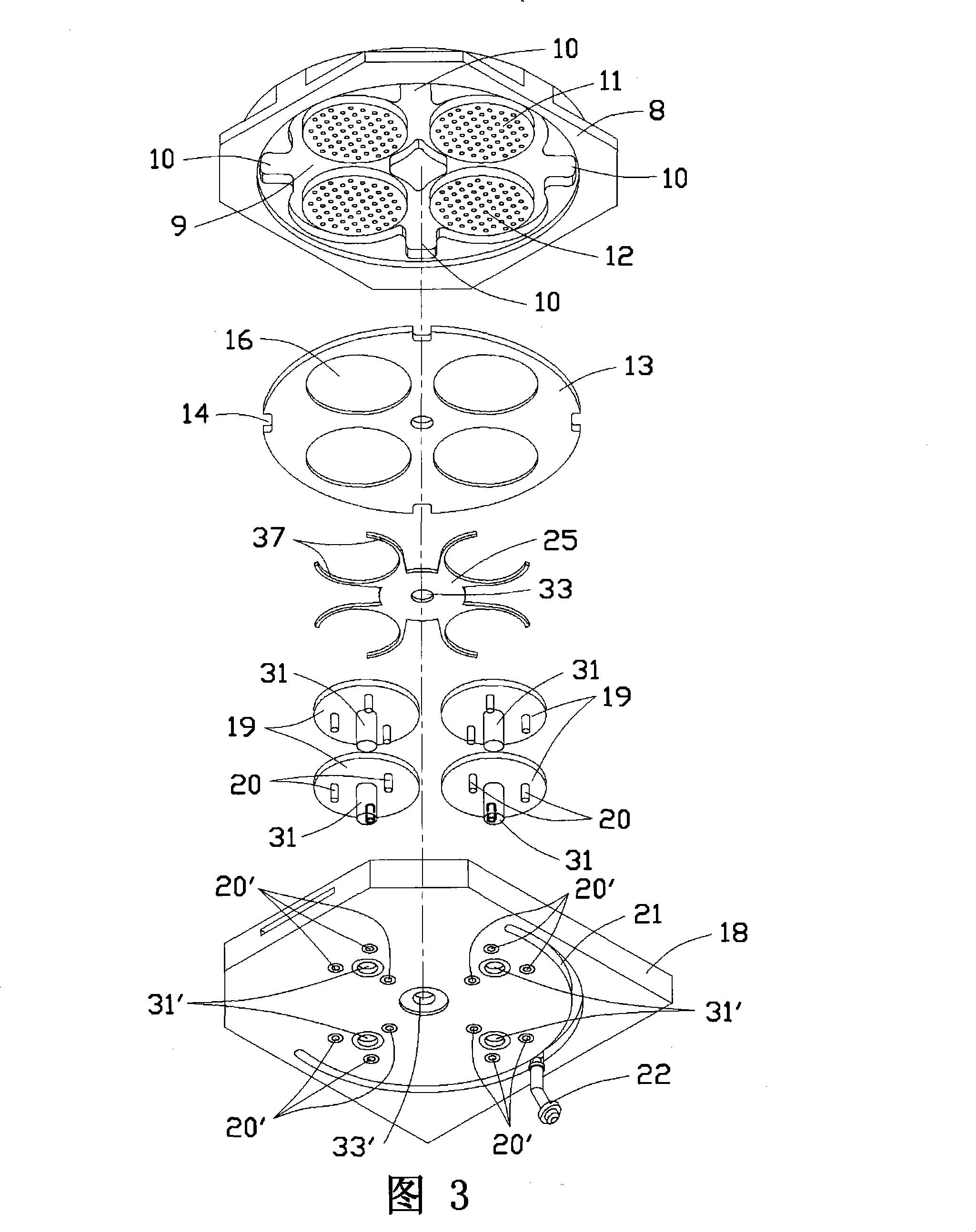
[0100]Please refer to FIG. 1 . FIG. 1 is a schematic perspective view of the semiconductor process system of the present invention. The present invention consists of a standard factory interface 1 , two vacuum locks 2 , a transfer chamber 3 , and one or more processing chambers 4 . Among them, the factory interface 1 is adjacent to the vacuum lock 2 . The transfer chamber 3 is located between the vacuum lock 2 and the processing chamber 4 . A plurality of processing chambers 4 may be arranged around the transfer chamber 3 . Each processing chamber 4 contains a plurality of processing platforms 5 , and each processing platform 5 can process a piece of semiconductor process. In the embodiment shown in FIG. 1 , the semiconductor processing system includes two processing chambers 4 arranged around the transfer chamber 3 . A chamber top cover 8 is arranged above each processing chamber 4. For the convenience of description of the present invention, the chamber top cover 8 of one...


PUM


Abstract

The invention relates to a semiconductor craft processing system, which comprises a vacuum lock, a transfer chamber, a processing cavity chamber or a plurality of processing cavity chambers; wherein, the transfer chamber is positioned between the vacuum lock and the processing cavity chamber, the processing cavity chamber can be arranged around the transfer chamber; a transfer device is arranged in the transfer chamber. The invention can adjust the position only through the movement of the transfer device, but the vacuum lock or the processing cavity chamber is not required in the vertical direction, the assembly and disassembly or the exchange motion of a craft piece can be accomplished, thereby the craft piece can be assemble, disassemble and exchanged rapidly and low-costly, and the production capacity is improved. The invention also discloses a processing cavity chamber of an intake and exhaust system which adopts a special design to lead a reaction gas curtain barrier to be formed between each processing platform in the processing cavity chamber, the homogeneity between each processing platform can be promoted, and the interference of the reaction gases between the different processing platforms is avoided.

Description

[0001] This case is a divisional application of a patent application with the application number 200510028562.8 and the filing date of August 5, 2005, entitled "Semiconductor Process Processing System and Its Processing Method". technical field [0002] The present invention relates to the technical field of semiconductor manufacturing equipment, in particular to a semiconductor process processing system and a processing method thereof. Background technique [0003] At present, there are two commonly used semiconductor process processing systems, one is a system for batch processing of process parts, and the other is for single-chip processing of process parts. In batch processing systems, multiple process pieces are placed horizontally or vertically and processed simultaneously. [0004] Since multiple process pieces are processed simultaneously in the device, the distance between process pieces is extremely limited. This requires low-pressure processing to eliminate gas p...

Claims


Application Information

Patent Timeline
IPC IPC(8): H01L21/00H01L21/02H01L21/67
Inventor 陈爱华
Owner ADVANCED MICRO FAB EQUIP INC CHINA
Why Eureka
Try Eureka