
Colour active matrix displays

An active matrix and color technology, applied in the field of color active matrix display equipment, can solve the problems that are not suitable for forming displays, etc., and achieve the effect of simple unit formation process

Active Publication Date: 2008-05-07
HYDIS TECH
View PDF0 Cites 3 Cited by
  • Summary
  • Abstract
  • Description
  • Claims
  • Application Information

AI Technical Summary

Problems solved by technology

This process is not suitable for forming displays because the etch holes are scattered across the array

Method used


Image

  • Colour active matrix displays
  • Colour active matrix displays
  • Colour active matrix displays

Examples


Embodiment Construction

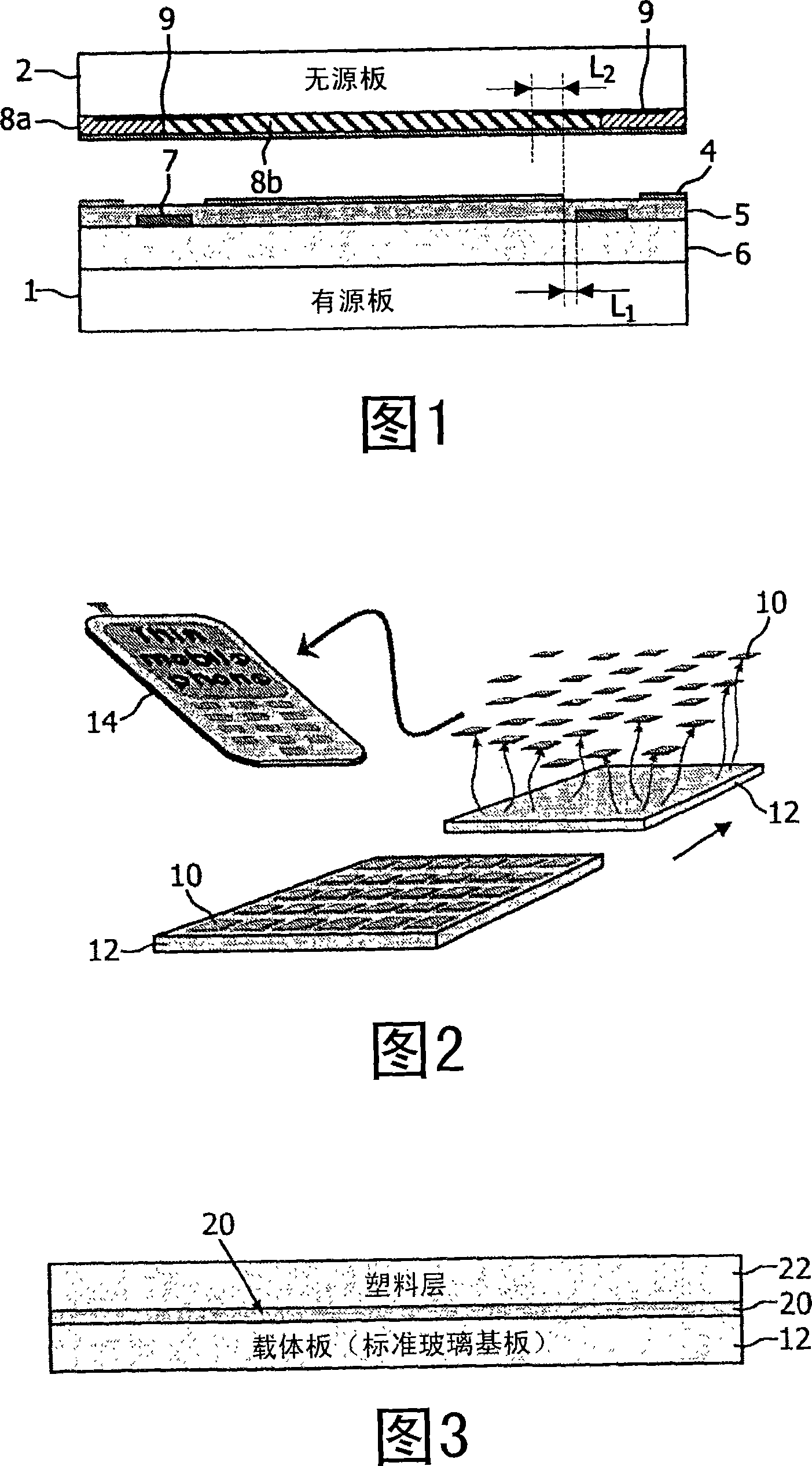
[0062] Figure 2 schematically shows the manufacture of a (not yet published) plastic display proposed by the applicant, showing the final separation stage. The completed display 10 is separated from the glass substrate 12 and subsequently used in a device such as a mobile phone 14 .

[0063] Figure 3 is used to explain the basic manufacturing concept and shows a glass carrier plate 12 with an a-Si separation layer 20 and a plastic layer 22 which acts as a plastic substrate. This substrate structure can form the basis for active and passive boards. FIG. 3 only shows one display substrate, but actually there will be many display units on the large glass substrate, as shown in FIG. 2 .

[0064] The separation layer 20 may be a thin layer of a-Si, which is deposited on the glass substrate 12 before adding the plastic layer 22 . The a-Si separation layer is applied by PECVD, for example, and may have a thickness of 10 to 50 nm. A laser separation process can be used to activate ...


PUM

PropertyMeasurementUnit
Thicknessaaaaaaaaaa

Abstract

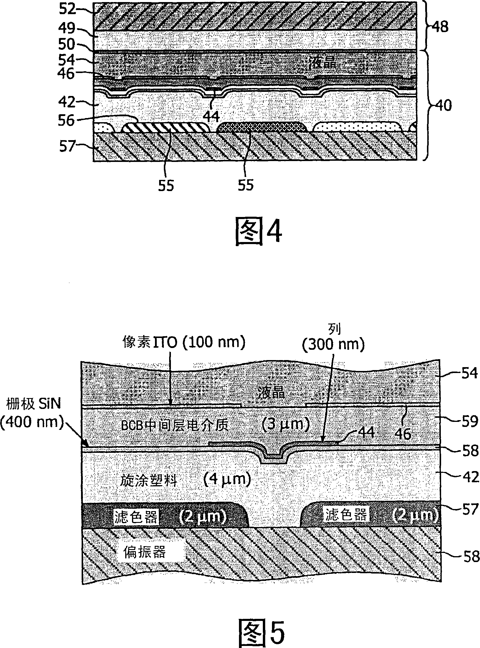
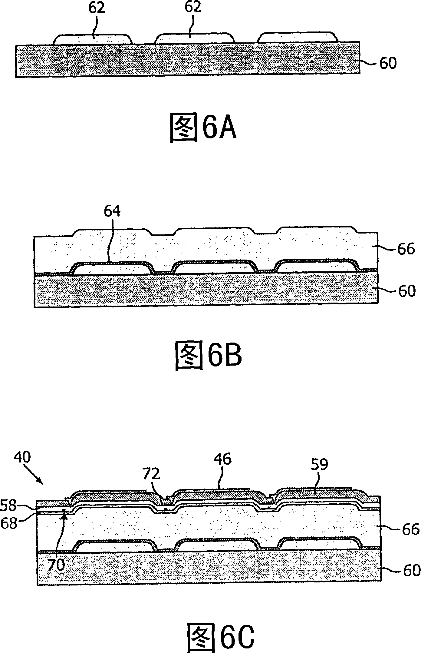
A method of manufacturing a colour active matrix display device comprises forming islands over a rigid carrier substrate, forming a plastic substrate over the rigid carrier substrate, forming an array of pixel circuits over the plastic substrate and forming a display layer over the array of pixel circuits. The rigid carrier substrate is then released from the plastic substrate and the plastic substrate then has channels defined by the islands. These are filled to define colour filter portions. The formation of a plastic substrate on a rigid carrier, with the use of a subsequent lift off process, enables the circuit arrays to be made on very thin plastic sheets. The colour filters can then be made on the outside of the LC cell. Depressions are formed in the plastic substrate registered to the circuit array, and these are filled in with colour filter material, for example by ink jet printing.

Description

technical field [0001] The present invention relates to color active matrix display devices, and in particular to the use of plastic substrates for the manufacture of such devices. Background technique [0002] The most common form of active matrix display is the active matrix liquid crystal display (AMLCD). AMLCD devices are often fabricated on large glass substrates 0.7mm thick. Two plates are required for one unit so that the finished display is just over 1.4mm thick. Manufacturers of mobile phones and some laptops need thinner and lighter displays, and the finished units can be thinned in HF (hydrofluoric acid) solution, usually to about 0.8mm thick. Mobile phone manufacturers ideally require displays to be even thinner, but have found that cells below 0.8mm thick made by this method are too fragile. [0003] HF thinning is unattractive because it is a wasteful process using hazardous chemicals that are difficult to dispose of safely and economically. There is also s...

Claims


Application Information

Patent Timeline
IPC IPC(8): G02F1/1335G02F1/1362G02F1/1333
CPCG02F1/1368G02F2001/133567H01L27/1266G02F1/133516G02F1/133305H01L27/322H01L27/1214G02F1/133567H10K59/38G02F1/1335G02B5/20
Inventor I·D·弗伦奇M·J·蔡尔兹D·A·菲什J·R·赫克托
Owner HYDIS TECH
Learn More