Exhaust air system, semi-conductor manufacturing installation for manufacturing thin film by the same and method thereof

A technology for manufacturing devices and semiconductors, which is applied in the field of chemical vapor deposition equipment, and can solve the problems of cleaning efficiency and reduced productivity of semiconductor manufacturing devices.

Inactive Publication Date: 2008-05-14
TES CO LTD
View PDF0 Cites 14 Cited by
  • Summary
  • Abstract
  • Description
  • Claims
  • Application Information

AI Technical Summary

Problems solved by technology

Therefore, the cleaning efficiency of the chamber and the productivity of the semiconductor manufacturing equipment will decrease

Method used


Image

  • Exhaust air system, semi-conductor manufacturing installation for manufacturing thin film by the same and method thereof
  • Exhaust air system, semi-conductor manufacturing installation for manufacturing thin film by the same and method thereof
  • Exhaust air system, semi-conductor manufacturing installation for manufacturing thin film by the same and method thereof

Examples


Embodiment Construction

[0052] In the drawings, like elements are numbered with like numbers.

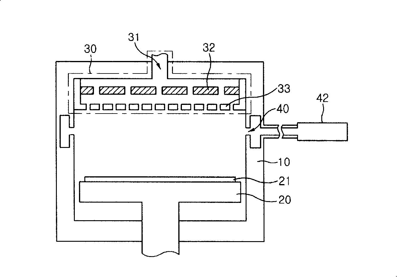
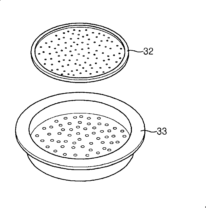
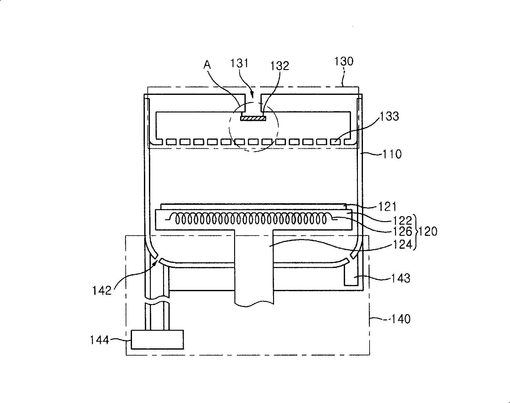
[0053] image 3 According to an embodiment of the present invention, a conceptual cross-sectional view of a semiconductor manufacturing device is drawn, Figure 4 is displayed image 3 A magnified view of part A of the Figures 5A to 5E 6A to 6C are conceptual cross-sectional views illustrating baffles according to an embodiment of the present invention, Figure 7 is a conceptual schematic diagram illustrating a pump interface according to an embodiment of the present invention.

[0054] Please refer to Figure 3 to Figure 7 , the semiconductor manufacturing device of the present invention includes a chamber 110, a shower head unit 130, a heating block 120 and a pump interface 140, wherein the chamber 110 has a predefined reaction space and a predefined bottom curved surface, and the shower head unit 130 includes a gas supply hole baffle 132 combined with 131 to inject gas into chamber 110, heating bl...


PUM


Abstract

A semiconductor manufacture device and a film manufacture method with the device are provided. The semiconductor manufacture device comprises a chamber with preliminary defined reaction space and a nozzle element, which is used for injecting preliminary defined gas transmitted through a gas supply hole into the chamber. The nozzle element comprises a baffle board, a heating block and a pump interface. The baffle board and the gas supply hole are hanged together. The heating block is under the nozzle element so that a wafer can be placed over the heating block. The pump interface comprises a plurality of discharge ports. As high temperature control can be realized easily, a high temperature hard cover can be formed to improve the quality of the film. Besides, the reaction gas can be evenly distributed on the nozzle and travel through the nozzle and be quickly injected into the substrate of the heater by using the baffle board, which is hanged together with the gas supply hole. Further more, the time taken by the reaction gas to travel through the nozzle and reach the substrate is minimized, which in turn minimizes the time to stabilize the reaction temperature. In addition, maintenance time and cost of the device are reduced.

Description

technical field [0001] The present invention relates to an exhaust system and a semiconductor manufacturing apparatus and method for manufacturing thin films using the system, and more particularly to a chemical vapor deposition (CVD) apparatus having an increased size, which can stably High temperature control is performed accurately and process gas can be introduced and discharged stably. Background technique [0002] In general, energy-sensitive photosensitive films are utilized as semiconductor element patterns become finer to maximize output per unit wafer. However, since diffused reflected light is generated due to the material layer under the photosensitive film, an anti-reflection coating (ARC) process using a nitride film is performed to prevent the diffused reflected light. Furthermore, because of the gradual increase in wafer size, wafers of 200 mm or larger are currently used. [0003] In at least one chamber, the large-sized wafer undergoes various processes r...

Claims


Application Information

Patent Timeline
Patent Type & Authority Applications(China)
IPC IPC(8): H01L21/00H01L21/205H01L21/3065C23C16/00C23C16/455C23F4/00H01J37/32H05H1/00
Inventor 朴根五
Owner TES CO LTD
Why Eureka
Try Eureka