Large area VHF-PECVD reaction chamber back feed-in type parallel plate electrode capable of obtaining even electric field

A uniform electric field and parallel plate technology, applied in gaseous chemical plating, metal material coating process, coating, etc., can solve problems such as plasma inhomogeneity, improve the uniformity of electric field distribution, and solve the uniformity of potential distribution Sexual problems, the effect of suppressing the potential standing wave effect

Inactive Publication Date: 2008-05-28
NANKAI UNIV
View PDF0 Cites 27 Cited by
  • Summary
  • Abstract
  • Description
  • Claims
  • Application Information

AI Technical Summary

Problems solved by technology

This electrode and power feeding method can obtain a practical large-area VHF-PECVD reaction chamber to solve the problem of plasma non-uniformity caused by non-uniform distribution of electric field, thereby promoting the industrialization of low-cost silicon thin film solar cells process

Method used


Image

  • Large area VHF-PECVD reaction chamber back feed-in type parallel plate electrode capable of obtaining even electric field
  • Large area VHF-PECVD reaction chamber back feed-in type parallel plate electrode capable of obtaining even electric field
  • Large area VHF-PECVD reaction chamber back feed-in type parallel plate electrode capable of obtaining even electric field

Examples


Embodiment 1

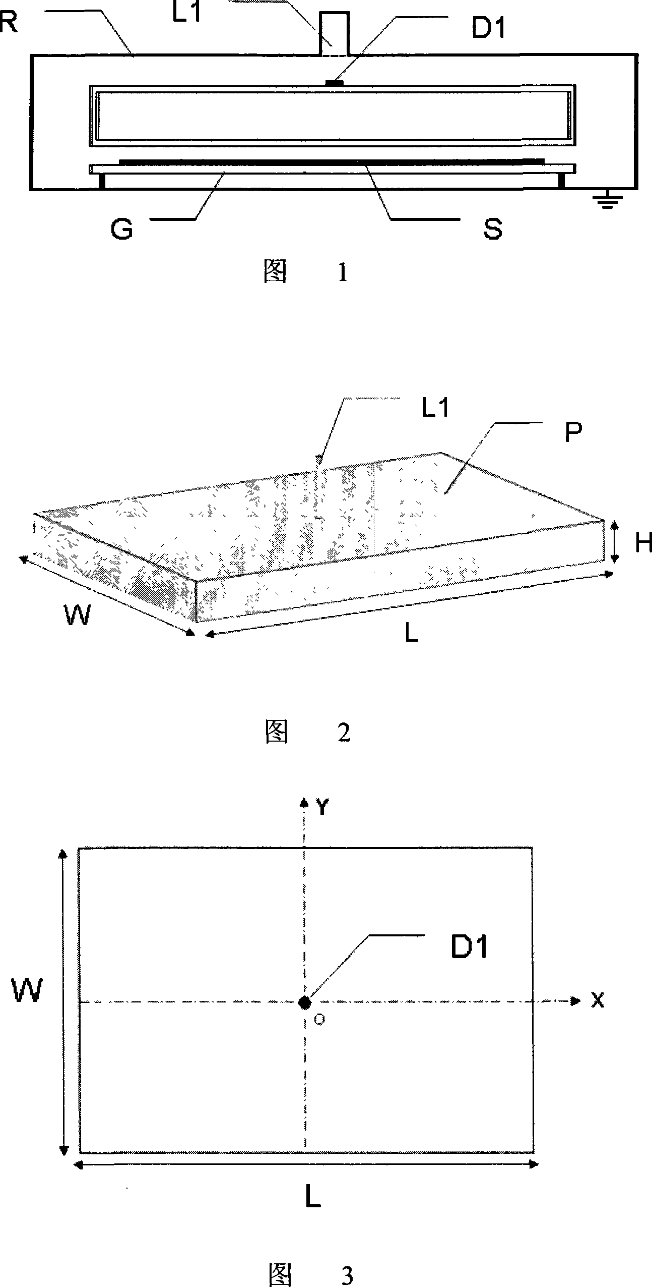
[0042] Back-fed parallel plate electrode single-point central power feed structure (as shown in Figure 2)

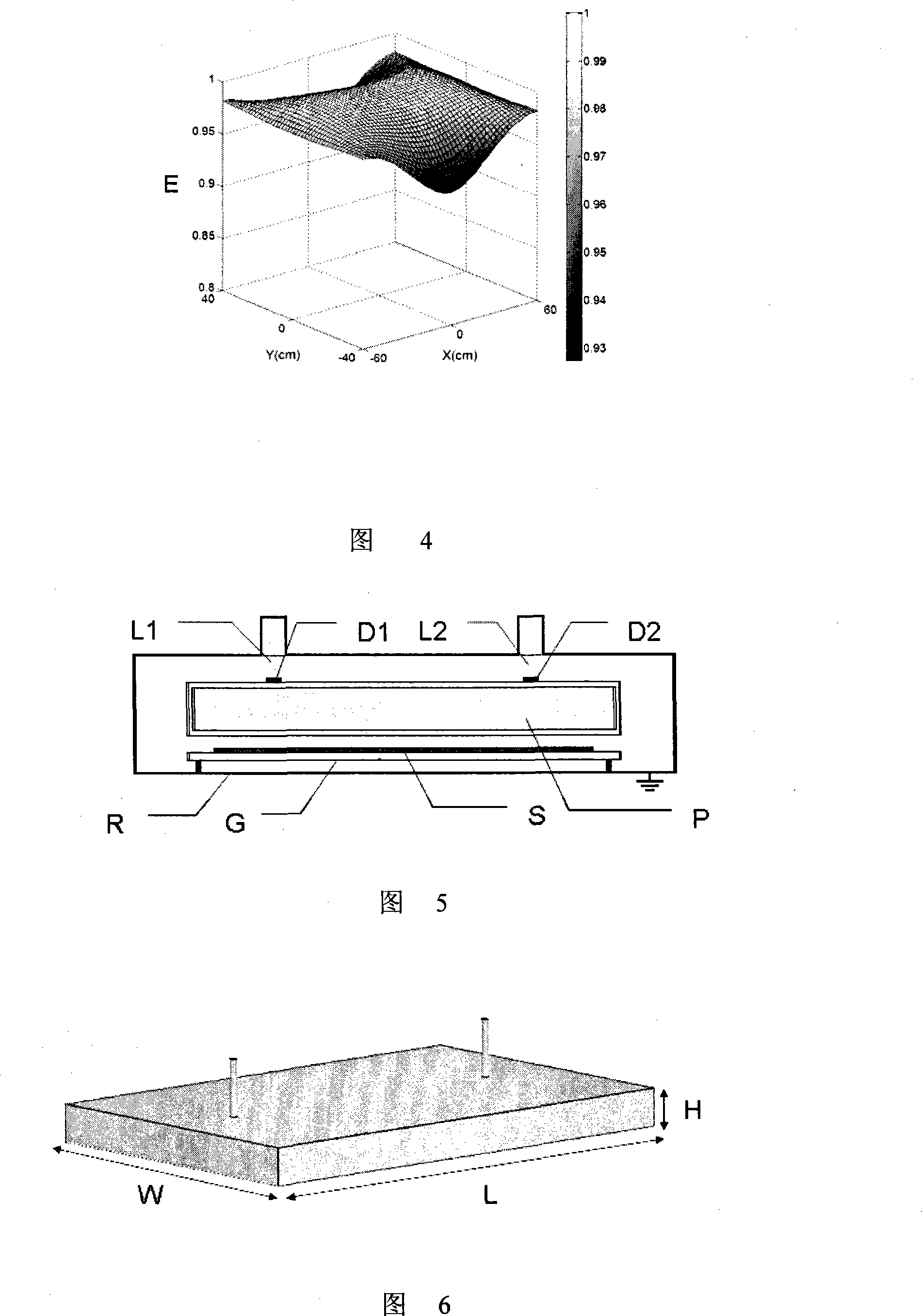
[0043] In this example, the rectangular parallel plate electrode has a length L=120cm, a width W=80cm, and a height H=10cm. The rear-side single-point feeding is adopted, and the electrode structure is shown in FIG. 1 of the embodiment. The position of the power feed-in point is shown in Figure 3, and the feed-in point D1 is located in the center of the x-y plane. The PECVD reaction chamber with the back-fed parallel plate electrode structure designed in this example is applied with a 40.68MHz excitation frequency power supply. The theoretical calculation results of the electric field distribution between the electrodes are shown in Figure 4, and the electric field non-uniformity is within ±4%. .

Embodiment 2

[0045] Two-point Power Feed-in (I) Structure of Back-fed Parallel Plate Electrodes

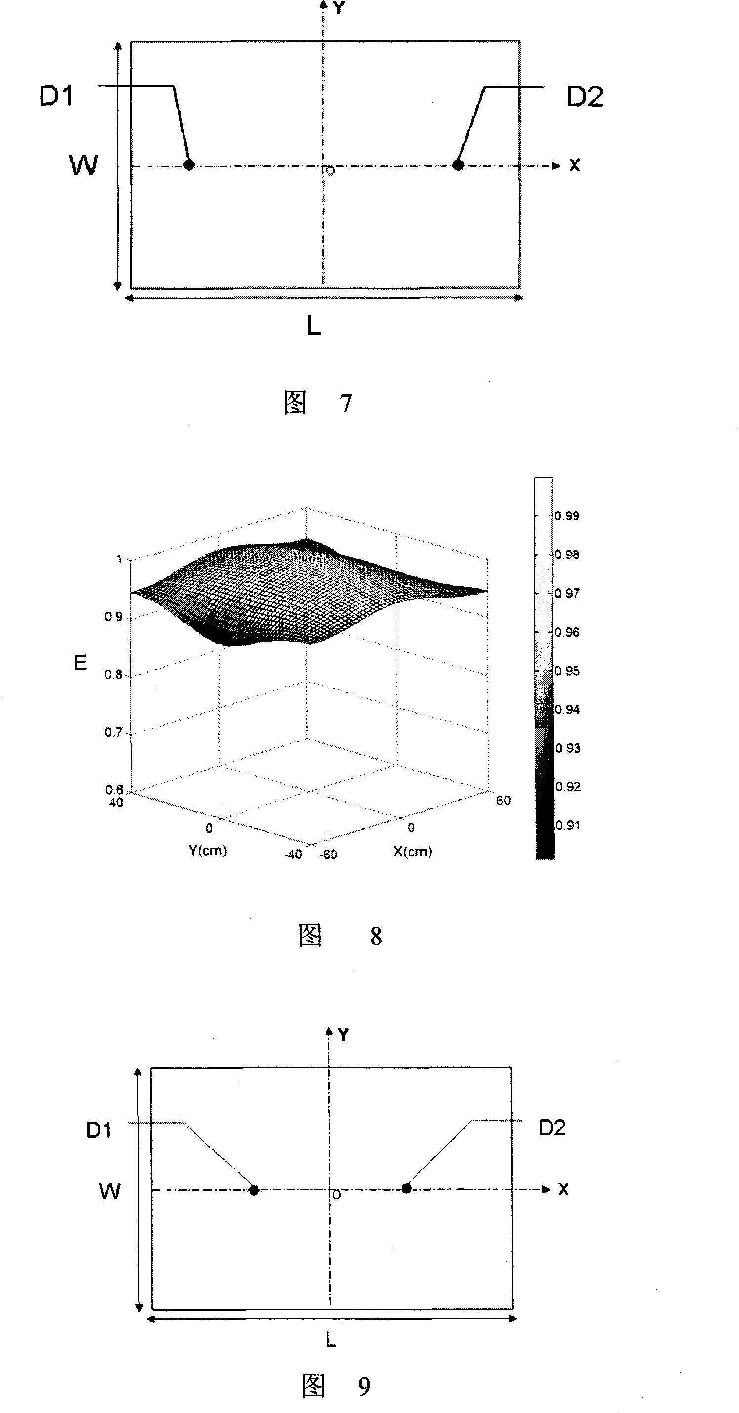
[0046] In this example, the rectangular parallel plate electrode has a length L=120cm, a width W=80cm, and a height H=10cm. The rear-side two-point feeding is adopted. The electrode structure is shown in Figure 6. The position of the power feed-in point is shown in Figure 7, and the x-y plane Cartesian coordinates of the feed-in points D1 and D2 are (40cm, 0) and (-40cm, 0) respectively. The PECVD reaction chamber with the back-fed parallel plate electrode structure designed in this example is applied with a 40.68MHz excitation frequency power supply, and the two ends are fed in with equal phase and equal amplitude power. The theoretical calculation results of the electric field distribution between the electrodes are shown in Figure 8. , the electric field non-uniformity is within ±5%.

Embodiment 3

[0048] Back-feed parallel plate electrode two-point power feed (II) structure

[0049] In this example, the rectangular parallel plate electrode has a length L=120cm, a width W=80cm, and a height H=10cm. The rear-side two-point feeding is adopted. The electrode structure is shown in Figure 6. The position of the power feeding point is shown in Figure 9, and the x-y plane Cartesian coordinates of the feeding points D1 and D2 are (25cm, 0) and (-25cm, 0) respectively. The PECVD reaction chamber with the back-fed parallel plate electrode structure designed in this example is applied with excitation frequency power supplies of 40.68MHz and 54.24MHz respectively, and the two ends are fed in with equal phase and equal amplitude power. The theoretical calculation results of the electric field distribution between the electrodes are as follows: As shown in Figures 10 and 11, the electric field non-uniformity is within ±2.5% and ±4.6%.


PUM


Abstract

The invention discloses a back feed-in parallel plate power electrode capable of achieving a large-area reaction chamber of VHF-PECVD with uniform electric fields, which includes a parallel plate power electrode plate and a power feed-in connection port and is characterized in that the power feed-in connection port is positioned on the back side of the power electrode plate of which the front face is opposite to a substrate S. The invention employs optimized distribution of the position of the electric power feed-in port to suppress logarithm singular point effect and standing wave effect of electric potential near the electrode feed-in port, ensuring great improvement of the uniformity of electric field distribution, thereby being capable of avoiding the problem that electric field distribution is uneven due to the employment of feed-in mode of electrode edge power. The invention resolves the problem of uniformity of electric potential distribution of the large-area electrode plate, which lays the groundwork for the research and development of thin films deposition and etching systems of the large-area VHF-PECVD and can powerfully promote industrialization process of matrix technique of silicon thin film solar cells and thin film transistors.

Description

【Technical field】 [0001] The invention relates to the technical field of thin-film transistor matrix in the field of silicon thin-film solar cells and flat panel displays, in particular to a large-area VHF-PECVD reaction chamber that can obtain a uniform electric field in a plasma-enhanced chemical vapor deposition or plasma etching reaction chamber electrode design. 【Background technique】 [0002] In recent years, it has been reported that the application of very high frequency (VHF) technology to PECVD can increase the deposition rate of thin films, and the research results show that: VHF-PECVD is completely suitable for high-speed deposition of microcrystalline silicon thin films and amorphous silicon thin films. However, the application research of VHF-PECVD is usually carried out in small-scale PECVD reaction chambers, so it cannot be directly applied to large-scale industrial production. RF capacitively coupled parallel plate electrode reaction chamber is widely used ...

Claims


Application Information

Patent Timeline
Patent Type & Authority Applications(China)
IPC IPC(8): C23C16/505
Inventor 赵颖张晓丹葛洪任慧志薛俊明许盛之张建军魏长春侯国付耿新华熊绍珍
Owner NANKAI UNIV
Why Eureka
Try Eureka