Camera and image processing method

A camera device and image processing technology, applied in image communication, brightness and chrominance signal processing circuits, signal generators with a single pick-up device, etc., can solve the problems of image resolution reduction, resolution reduction, image shrinkage, etc. , to achieve the effect of improving noise and suppressing the decline of resolution

Inactive Publication Date: 2008-05-28
OLYMPUS CORP
View PDF1 Cites 13 Cited by
  • Summary
  • Abstract
  • Description
  • Claims
  • Application Information

AI Technical Summary

Problems solved by technology

Therefore, although the noise is reduced, it also leads to a decrease in the resolution of the image
[0006] That is, the all-pixel image data obtained by reading out all the pixels has high resolution, but when the sensitivity becomes high, the noise le

Method used


Image

  • Camera and image processing method
  • Camera and image processing method
  • Camera and image processing method

Examples


no. 1 Embodiment approach

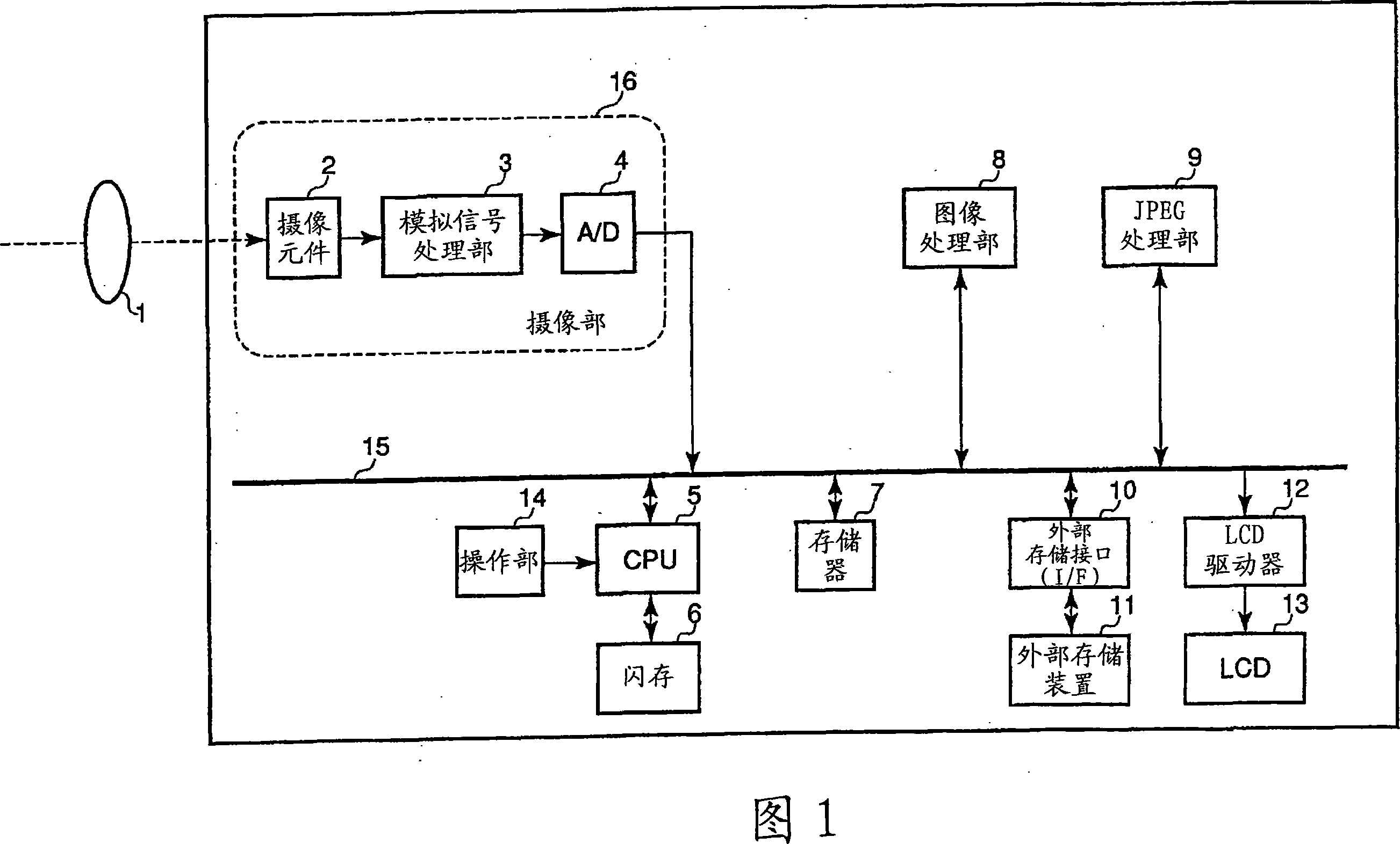
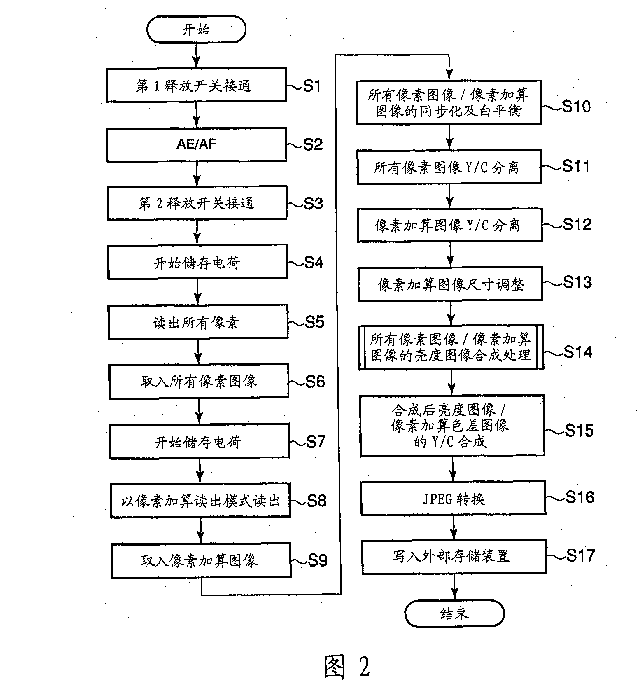
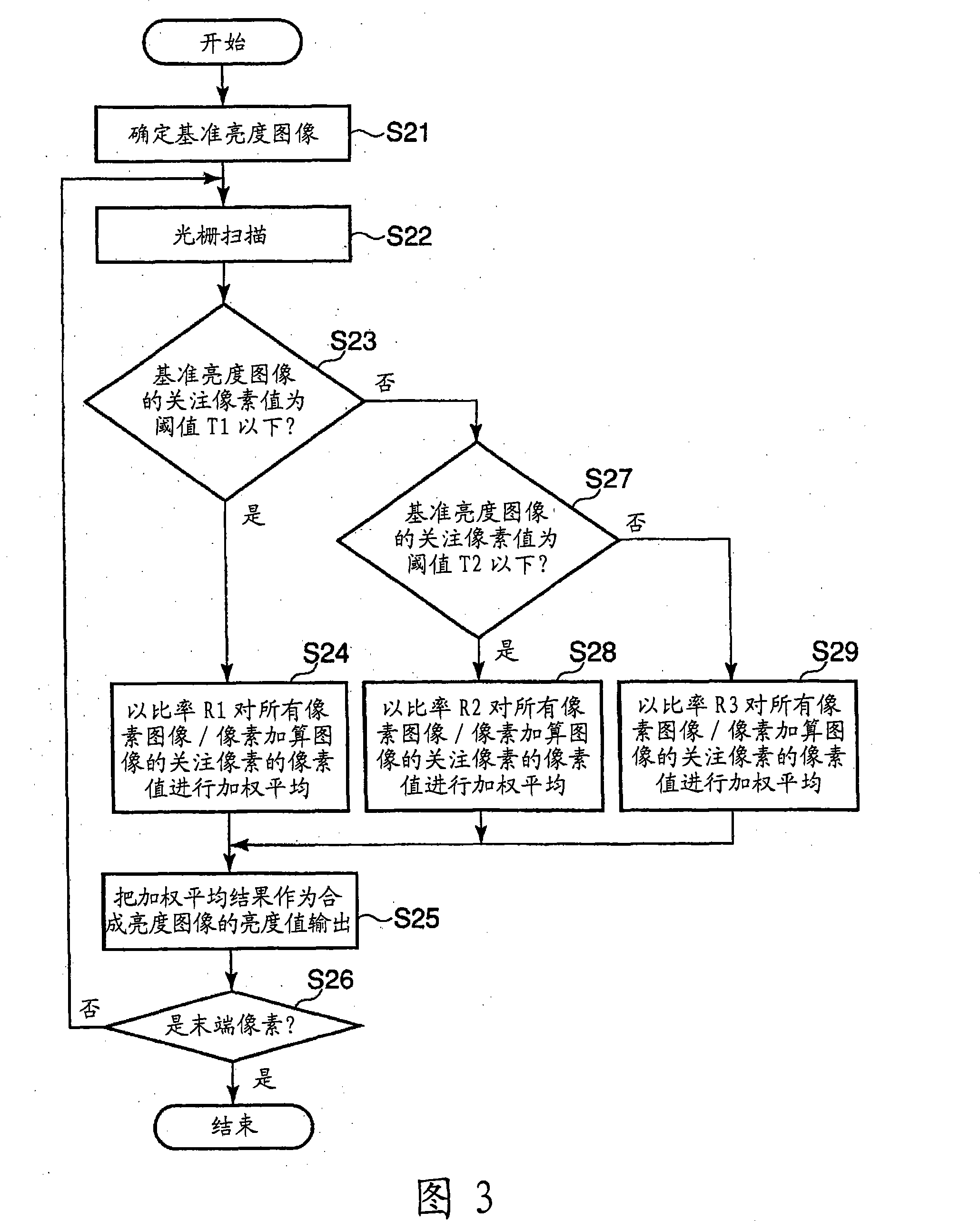
[0021] FIG. 1 is a block diagram showing the main configuration of the imaging device according to the first embodiment of the present invention. As shown in FIG. 1, the imaging device of this embodiment has a lens 1, an imaging element 2, an analog signal processing unit 3, an A / D conversion unit 4, a CPU 5, a flash memory 6, a memory 7, an image processing unit 8, and a JPEG processing unit 9. , An external storage interface (I / F) 10, an external storage device 11, an LCD driver 12, an LCD 13, an operating unit 14 and a bus 15. In addition, the imaging element 2, the analog signal processing unit 3, and the A / D conversion unit 4 constitute the imaging unit 16.

[0022] The lens 1 condenses light from a subject not shown. The imaging element 2 receives the light converged by the lens 1, converts it into electric charge corresponding to the amount of light received, and outputs the electric charge as an image signal. Here, if the imaging element 2 is an imaging element having an a...

no. 2 Embodiment approach

[0039] Next, the second embodiment of the present invention will be described. 4 is a block diagram showing the main configuration of an imaging device according to a second embodiment of the present invention. Here, the constituent elements assigned the same reference numerals in FIG. 4 as those in FIG. 1 are the same as those in FIG. 1, so the description is omitted. The imaging device shown in FIG. 4 is provided with an optical path branching prism 20. The optical path branching prism 20 branches the light converged by the lens 1 so that one of the branched lights enters the imaging unit 27 and the other light enters the imaging unit 28. According to this structure, the light from the subject can be incident on the two imaging units at the same time.

[0040] That is, the light converged by the lens 1 is divided into two systems by the optical path branching prism 20, and each light is received by the imaging element 21 and the imaging element 22. Here, the imaging element 21 h...


PUM


Abstract

The invention provides a videography device and an image processing method, thereby generating the image restraining the reduction of the resolving power and improving the illumination and color noise when in videography of high photographic sensibility. The image obtained synchronously based on all pixel read mode and the image based on the pixel tot read mode are separated into illumination ingredient and aberration ingredient, with self-adapting mixture treatment. All the pixel image data has the characteristic of high resolving power and the pixel tot image data has the characteristic of favorable illumination and color noise. In order to restrain the reduction of the resolving power and reduce the illumination noise, according to the illumination, the illumination ingredient of all pixel image data and the illumination ingredient of the pixel tot image data are weighted averaged, to generate the illumination ingredient image with favorable noise character and resolving power.

Description

Technical field [0001] The present invention relates to an imaging device, and in particular to an imaging device that can reduce noise in image data and an image processing method thereof. Background technique [0002] In all imaging devices represented by digital cameras, high-sensitivity photography is adopted as an imaging method in a low-illuminance environment. The high-sensitivity photography mentioned here refers to a method of using an amplifier to amplify the image signal output from the imaging element to obtain an image signal of the target intensity in a short time. In this kind of high-sensitivity photography, when shooting images with the same exposure, compared with low-sensitivity photography, it has the advantage that the exposure photography can be completed in a short time, but on the other hand, it has the following disadvantages, because it is stored in the imaging element The reduction in the amount of charge in the battery makes the signal component buried...

Claims


Application Information

Patent Timeline
IPC IPC(8): H04N9/04H04N9/77H04N5/335H04N5/347H04N5/357H04N5/369H04N5/378H04N9/07
Inventor 伊东觉
Owner OLYMPUS CORP
Why Eureka
Try Eureka