
Semiconductor integrated circuit and manufacturing method thereof

An integrated circuit and semiconductor technology, applied in the field of power integrated circuits and its production, can solve the problems of semiconductor integrated circuit reliability damage, power transistor damage, etc., and achieve the effect of improving reliability, low-cost manufacturing, and high-speed manufacturing

Inactive Publication Date: 2008-06-04
PANASONIC CORP
View PDF3 Cites 4 Cited by
  • Summary
  • Abstract
  • Description
  • Claims
  • Application Information

AI Technical Summary

Problems solved by technology

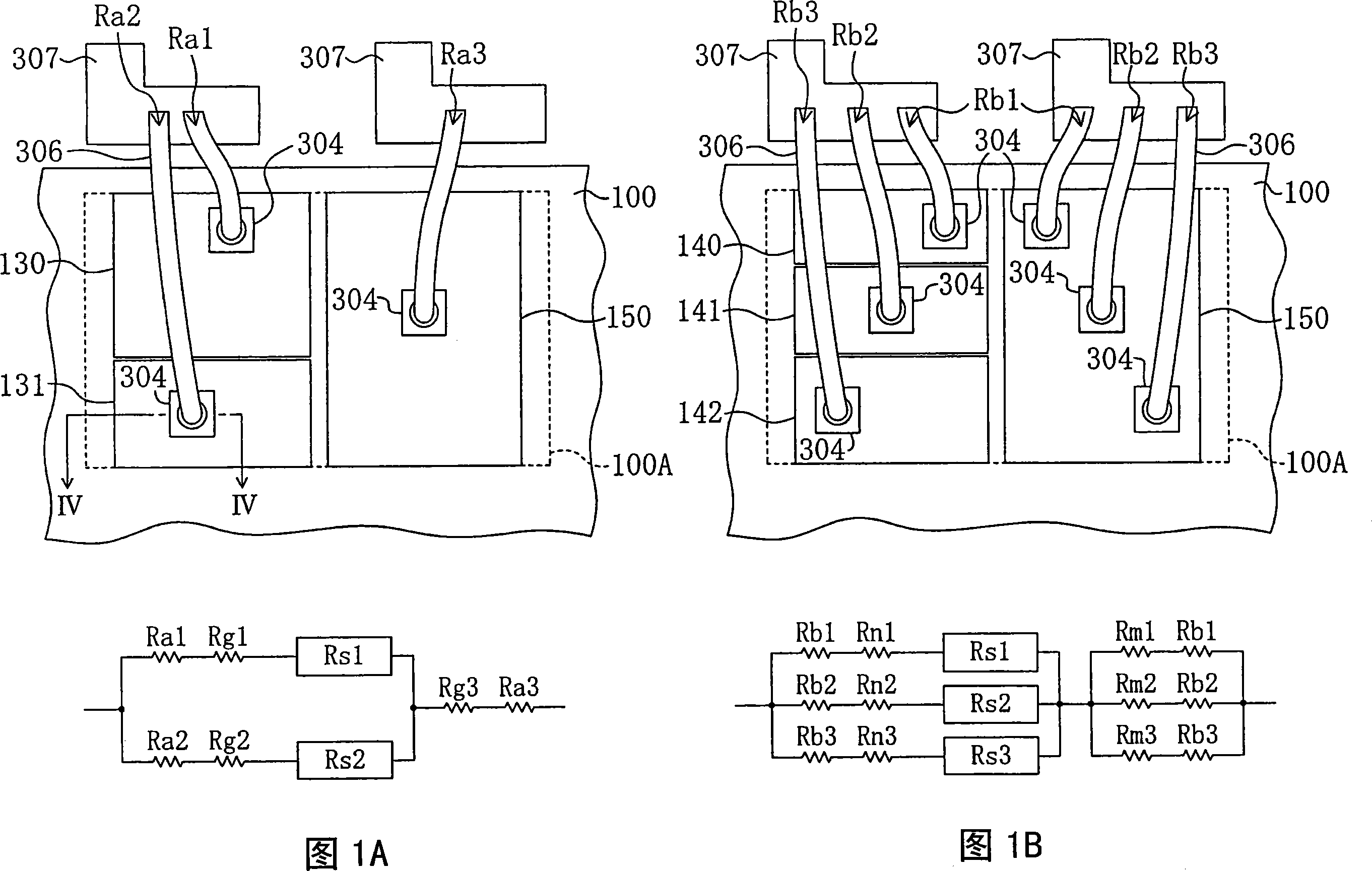
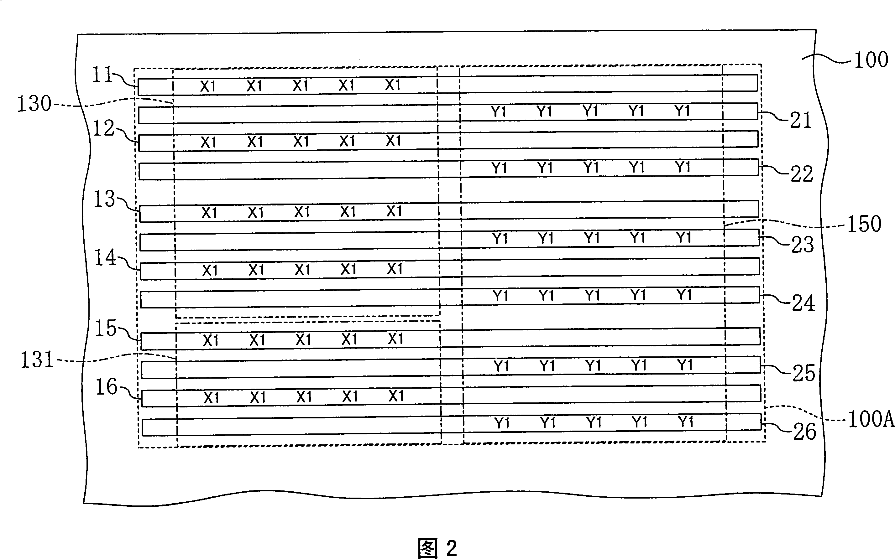
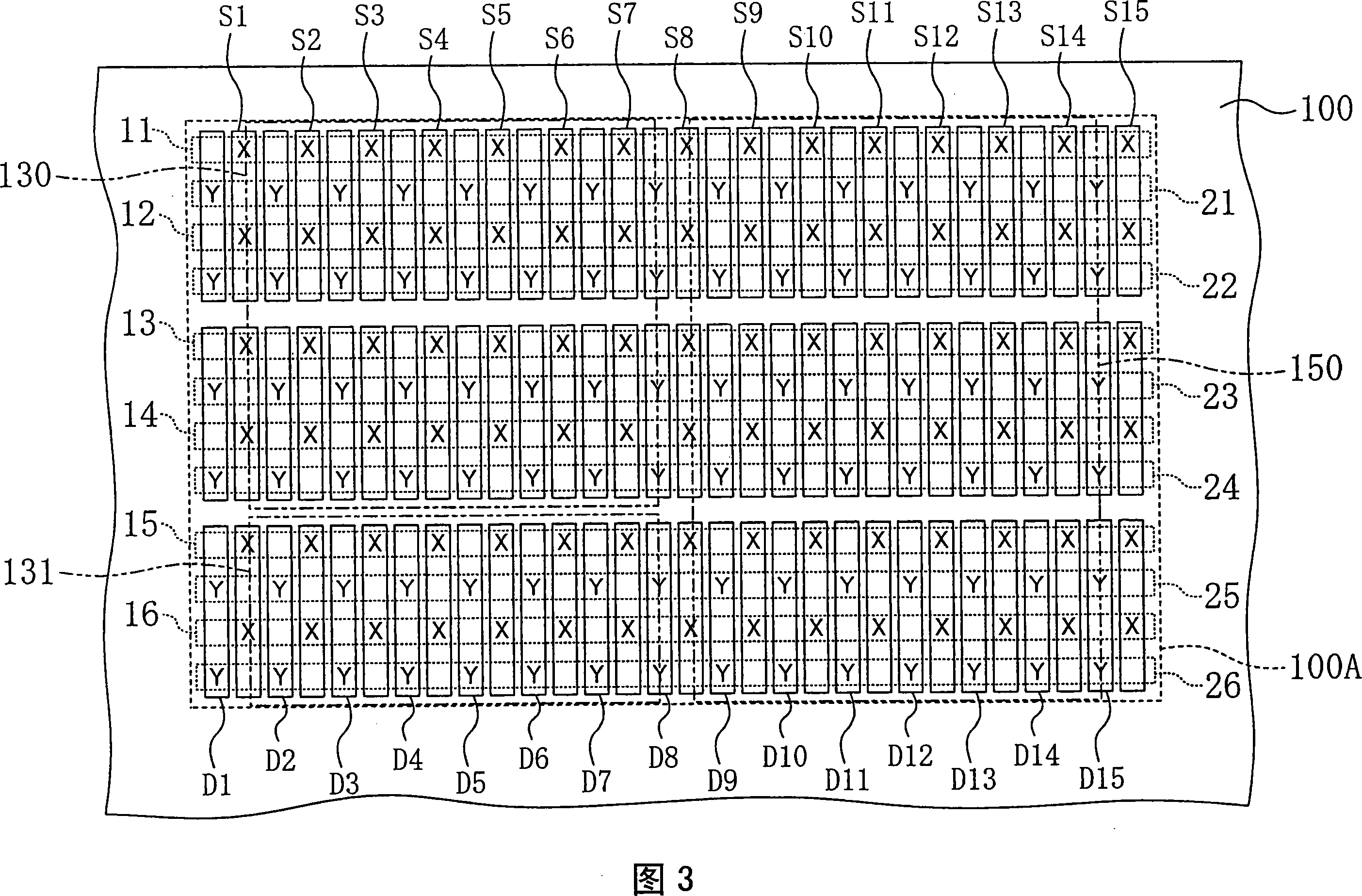
[0033] In addition, when a large current flows into the power transistor, because the bus lines connected to the source electrode and the drain electrode of the power transistor are connected to a plurality of common contact bosses, there are also power transistors (such as power NPN transistors, etc.) Depending on the type of the electrode, current concentration occurs in some layouts of the bus lines connected to the electrodes, causing damage to the power transistor and thus deteriorating the reliability of the semiconductor integrated circuit.

Method used


Image

  • Semiconductor integrated circuit and manufacturing method thereof
  • Semiconductor integrated circuit and manufacturing method thereof
  • Semiconductor integrated circuit and manufacturing method thereof

Examples


no. 2 Embodiment approach

[0138] Next, a semiconductor integrated circuit and a manufacturing method thereof according to a second embodiment of the present invention will be described with reference to the drawings.

[0139] 5 and the aforementioned FIG. 1( b ) respectively show a schematic plan view and an electrical circuit diagram of a part of the semiconductor integrated circuit according to the first embodiment of the present invention.

[0140] The common feature of the semiconductor integrated circuits shown in FIG. 5 and the above-mentioned FIG. 1 (b) is that they have a plurality of divided buses and a single bus, and the areas of the multiple buses are different from each other. Starting from one side of the frame, it is sequentially reduced as it gets farther away. In addition, since the structure of the semiconductor integrated circuit shown in FIG. 1(b) above has already been described in the first embodiment, the structure of the semiconductor integrated circuit shown in FIG. Some of th...

no. 3 Embodiment approach

[0166] Next, a semiconductor integrated circuit and a manufacturing method thereof according to a third embodiment of the present invention will be described with reference to the drawings.

[0167] 6( a ) and ( b ) each show a schematic plan view of a part of the semiconductor integrated circuit according to the third embodiment of the present invention.

[0168] The semiconductor integrated circuits shown in FIGS. 6( a ) and ( b ) have a common feature that they include a plurality of divided buses and a single bus, and the areas of the plurality of buses are equal to each other. In addition, in the following description about the structure of the semiconductor integrated circuit shown in FIGS. 6( a ) and ( b ), parts that overlap with those described in the first embodiment will be omitted.

[0169] In the semiconductor integrated circuit shown in FIG. 6(a), two bus lines 130, 131 are provided which are connected to the source electrodes and have the same area as each other...

no. 4 Embodiment approach

[0184] Next, a semiconductor integrated circuit and a manufacturing method thereof according to a third embodiment of the present invention will be described with reference to the drawings.

[0185] In the fourth embodiment, first to third modification examples that can be applied to the semiconductor integrated circuit according to the above-mentioned first to third embodiments will be described. In addition, as the description of the first to third modification examples, the semiconductor integrated circuit shown in FIGS. application as an example to describe.

[0186] Modification 1

[0187] The first modification shown in FIGS. 7( a ) and ( b ) is characterized in that the active regions of the power transistors are electrically separated from each other by separation layers.

[0188] Specifically, in FIG. 7(a), the active region of the power transistor is divided into two active regions 100a1 and 100a2, and in the two active regions 100a1 and 100a2, separated layers are...


PUM


Abstract

A semiconductor integrated circuit relating to one aspect of the present invention includes a power transistor, at least one or more of first metal patterns functioning as a first electrode of the power transistor and at least one or more of second metal patterns functioning as a second electrode of the power transistor formed in an interlayer insulation film on the transistor, at least one or more of first busses electrically connected to a corresponding first metal pattern of the at least one or more of the first metal patterns, a single second bus electrically connected to the at least one or more of second metal patterns, and a contact pad provided to each of the at least one or more of first busses and the single second bus.

Description

technical field [0001] The invention relates to a semiconductor integrated circuit and a manufacturing method thereof, in particular to the application of POE (Pad on Element) technology, that is, the technology of setting a boss (Pad) directly above (directly above) a semiconductor device, which can be directly above an active circuit area. A power integrated circuit with a wire bonding structure and a method for manufacturing the same. Background technique [0002] In recent years, with the popularization of information technology, there has been an increasing demand for higher speed and lower power consumption of electronic devices such as computers, information storage devices, mobile phones, and portable cameras. [0003] The factors that have a greater impact on the performance of these electronic devices include the backbone semiconductor electronic components such as power supplies, motor drivers, and audio amplifiers; and the factors that have a greater impact on th...

Claims


Application Information

Patent Timeline
Patent Type & Authority Applications(China)
IPC IPC(8): H01L27/04H01L23/522H01L23/485H01L21/822H01L21/768H01L21/60
CPCH01L27/088H01L2224/45124H01L2924/0105H01L2924/00014H01L2924/01045H01L2224/48699H01L2224/05567H01L2224/48091H01L2224/49171H01L2924/01013H01L24/49H01L2224/45015H01L24/48H01L24/06H01L2924/20753H01L2924/19043H01L2924/3011H01L2224/48247H01L2924/01033H01L2924/01074H01L2924/01078H01L2224/49111H01L2924/01015H01L2924/01082H01L2924/01004H01L21/823475H01L2224/49113H01L2924/20752H01L23/49562H01L2924/01327H01L2224/05553H01L23/4952H01L2924/01029H01L2224/05556H01L2924/014H01L2224/05571H01L2224/45147H01L24/03H01L2224/48599H01L2224/85399H01L2924/01079H01L2224/48465H01L24/05H01L2924/01037H01L2224/04042H01L2924/14H01L2224/48011H01L2924/01005H01L2924/01006H01L2924/20754H01L2224/05599H01L2924/01014H01L2224/45144H01L2224/48799H01L2924/13091H01L2224/02166H01L2224/0603H01L24/45H01L2924/20651H01L2924/00H01L2924/20755H01L2924/2075
Inventor 深水新吾锅岛有山本泰永
Owner PANASONIC CORP
Learn More