
Method for multi-exposure beam lithography device

A technology of electromagnetic radiation and actual position, which is applied in photoplate-making process exposure devices, microlithography exposure equipment, optics, etc., and can solve problems such as increased CD errors.

Active Publication Date: 2008-06-04
MICRONIC LASER SYST AB
View PDF2 Cites 3 Cited by
  • Summary
  • Abstract
  • Description
  • Claims
  • Application Information

AI Technical Summary

Problems solved by technology

[0007] It is therefore an object of the present invention to provide a method of patterning a workpiece which overcomes or at least reduces the above-mentioned problem of increased CD error when using a multi-beam pattern generator

Method used


Image

  • Method for multi-exposure beam lithography device
  • Method for multi-exposure beam lithography device
  • Method for multi-exposure beam lithography device

Examples


Embodiment Construction

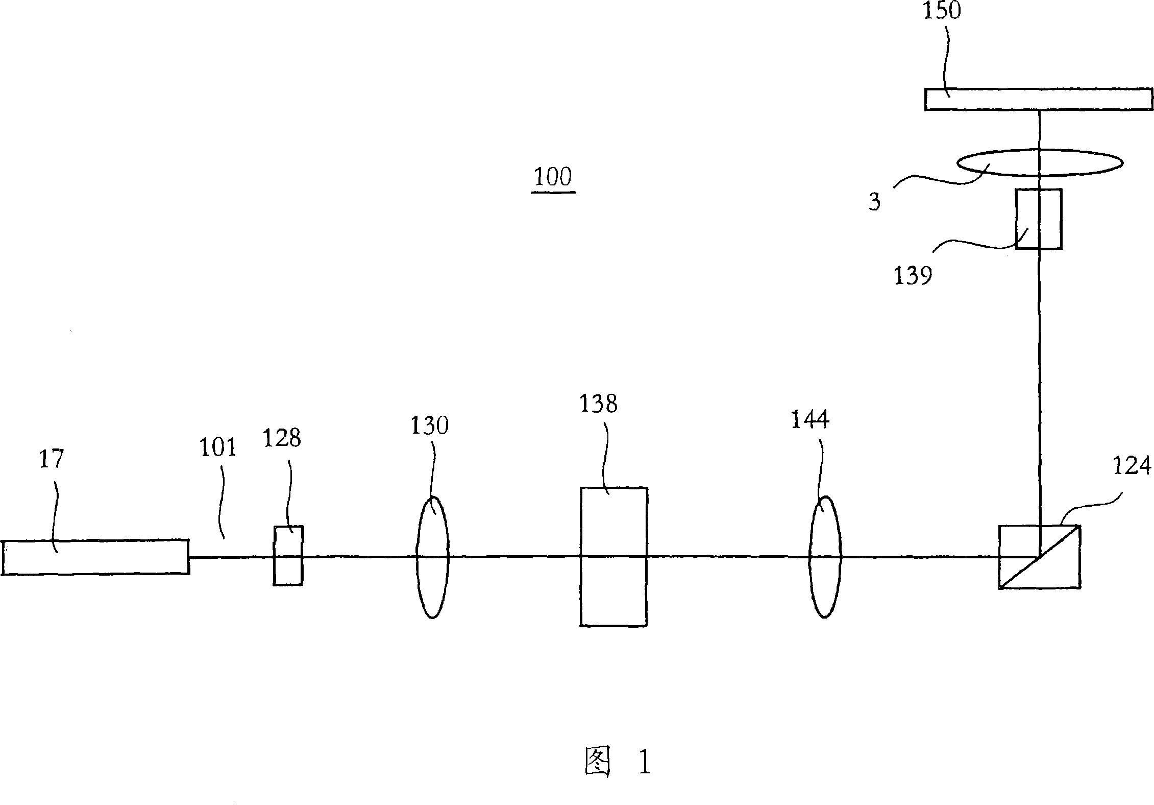
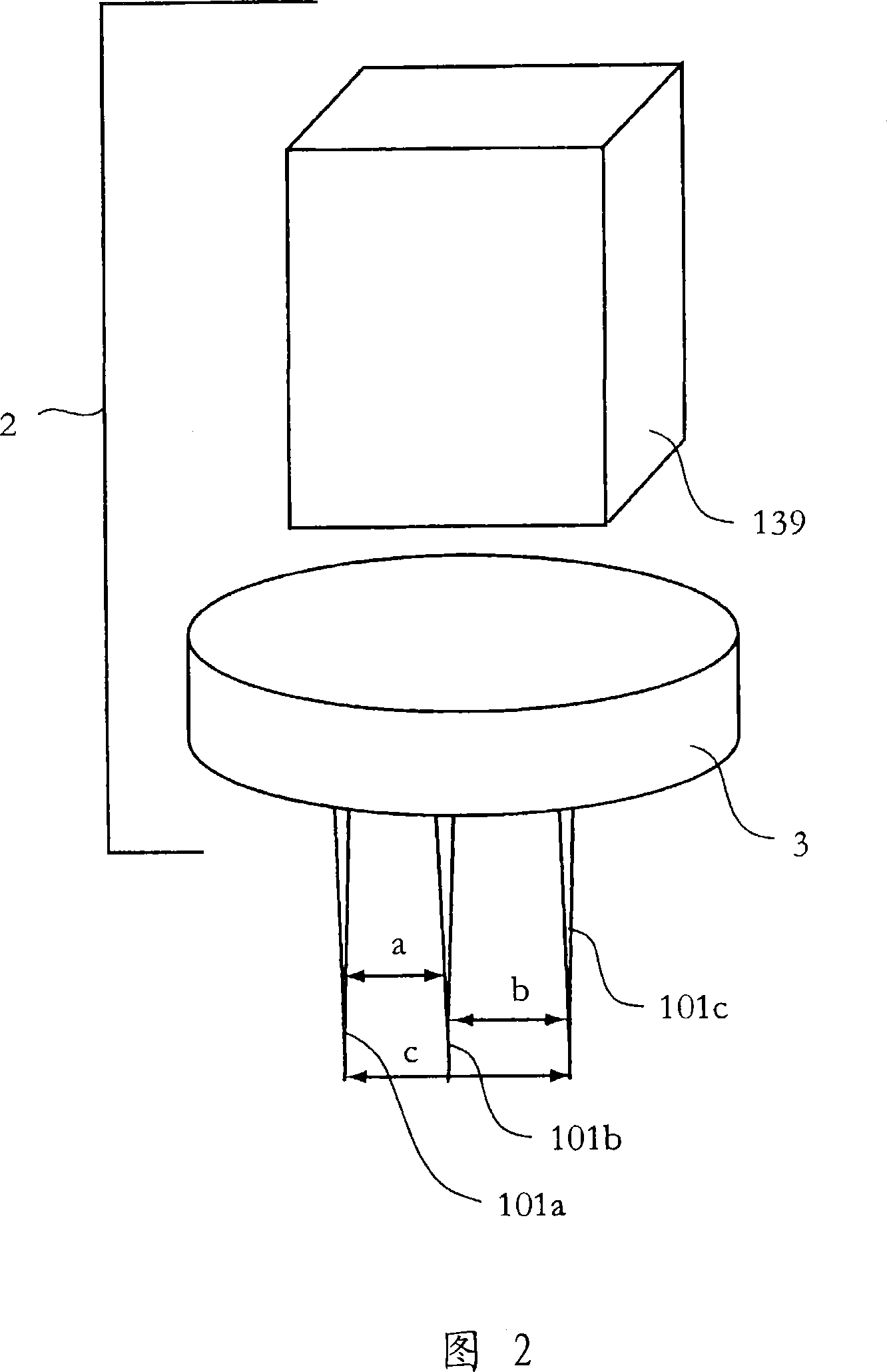
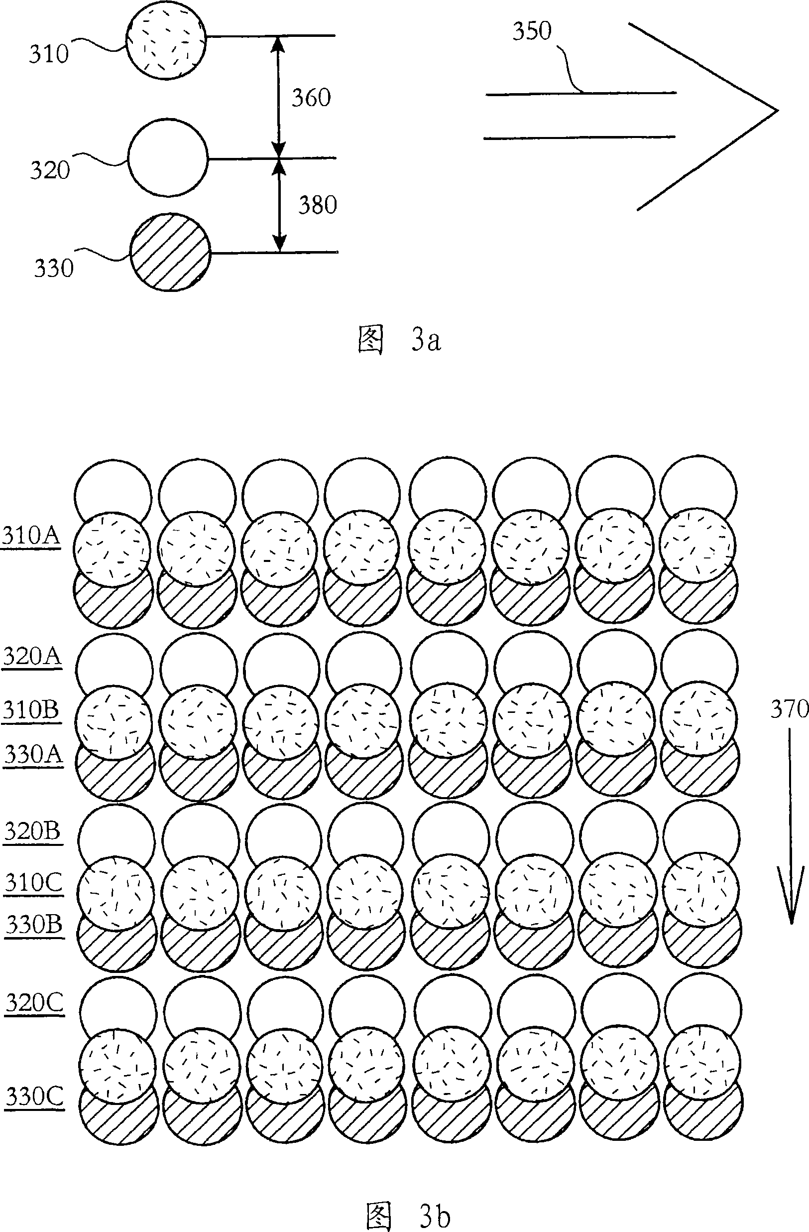
[0029] The present invention will be described in detail below with reference to the accompanying drawings. The preferred embodiments are described to explain the invention, not to limit the scope of the invention defined by the claims. Those of ordinary skill in the art will recognize many equivalent variations in the description that follows.

[0030] Further, the preferred embodiment is described with reference to a laser scanning pattern generator. It is obvious to those skilled in the art that any exposure means can be equally applied, such as light from IR to EUV, x-rays, or particle or atomic beams such as electrons and ions.

[0031] The invention is further described with reference to the production of masks or reticles, for example to produce periodic patterns on eg displays. It is obvious to those skilled in the art that the method and apparatus of the present invention are equally applicable to the direct writing of arbitrary patterns in masks, reticle displays o...


PUM

PropertyMeasurementUnit
wavelengthaaaaaaaaaa
lengthaaaaaaaaaa

Abstract

An aspect of the present invention includes a method for patterning a workpiece covered at least partly with a layer sensitive to electromagnetic radiation by simultaneosly using a plurality of exposure beams. In an example embodiement it is determined if any of the beams have an actual position relative to a reference beam which differs from its intended position. An adjustment of the exposure dose for a wrongly positioned beam is performed if said beam is printed at en edge of a feature. Other aspects of the present invention are reflected in the detailed description, figures and claims.

Description

technical field [0001] The present invention relates to a method for patterning a workpiece, in particular to a method of improving an image to be patterned on said workpiece by utilizing a plurality of exposure beams. Background technique [0002] Critical when generating periodic patterns on a mask or reticle for the production of e.g. A quality requirement is the absence of defects such as shade differences, light and dark fields, streaks or lines in the pattern. [0003] The deviations that cause these defects, such as CD (critical dimension) or positional errors, are usually very small, from hundreds of nanometers or less to less than one nanometer. This dimensional deviation, distributed over a relatively large area on a substrate, which may be 1500 x 1200 mm, such as a display photomask or a semiconductor wafer, can be very difficult, if not impossible, to detect by measurement. However, the human eye is very sensitive to systematic variations and can detect such sm...

Claims


Application Information

Patent Timeline
Patent Type & Authority Applications(China)
IPC IPC(8): G03F7/20
CPCG03F7/70383G03F7/70558G03F7/2053G03F7/70466
Inventor 弗雷德里克·肖斯特罗姆
Owner MICRONIC LASER SYST AB
Learn More