Photolithographic critical dimension control using reticle measurements

A technology of mastering and lithography, applied in the field of lithography, can solve problems such as unsatisfactory product manufacturing operations and no consideration of new mask bias

Inactive Publication Date: 2006-09-13
GLOBALFOUNDRIES INC
View PDF4 Cites 0 Cited by
  • Summary
  • Abstract
  • Description
  • Claims
  • Application Information

AI Technical Summary

Problems solved by technology

Typically, this feedback arrangement does not account for the new mask bias, and the resulting production run does not meet the figure 1 The design size specification is 160

Method used


Image

  • Photolithographic critical dimension control using reticle measurements
  • Photolithographic critical dimension control using reticle measurements
  • Photolithographic critical dimension control using reticle measurements

Examples


Embodiment Construction

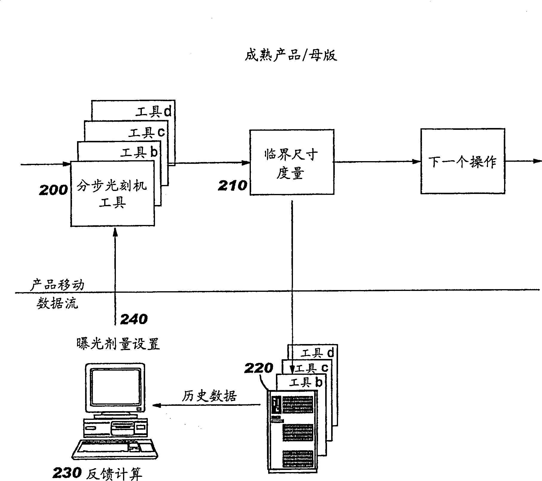
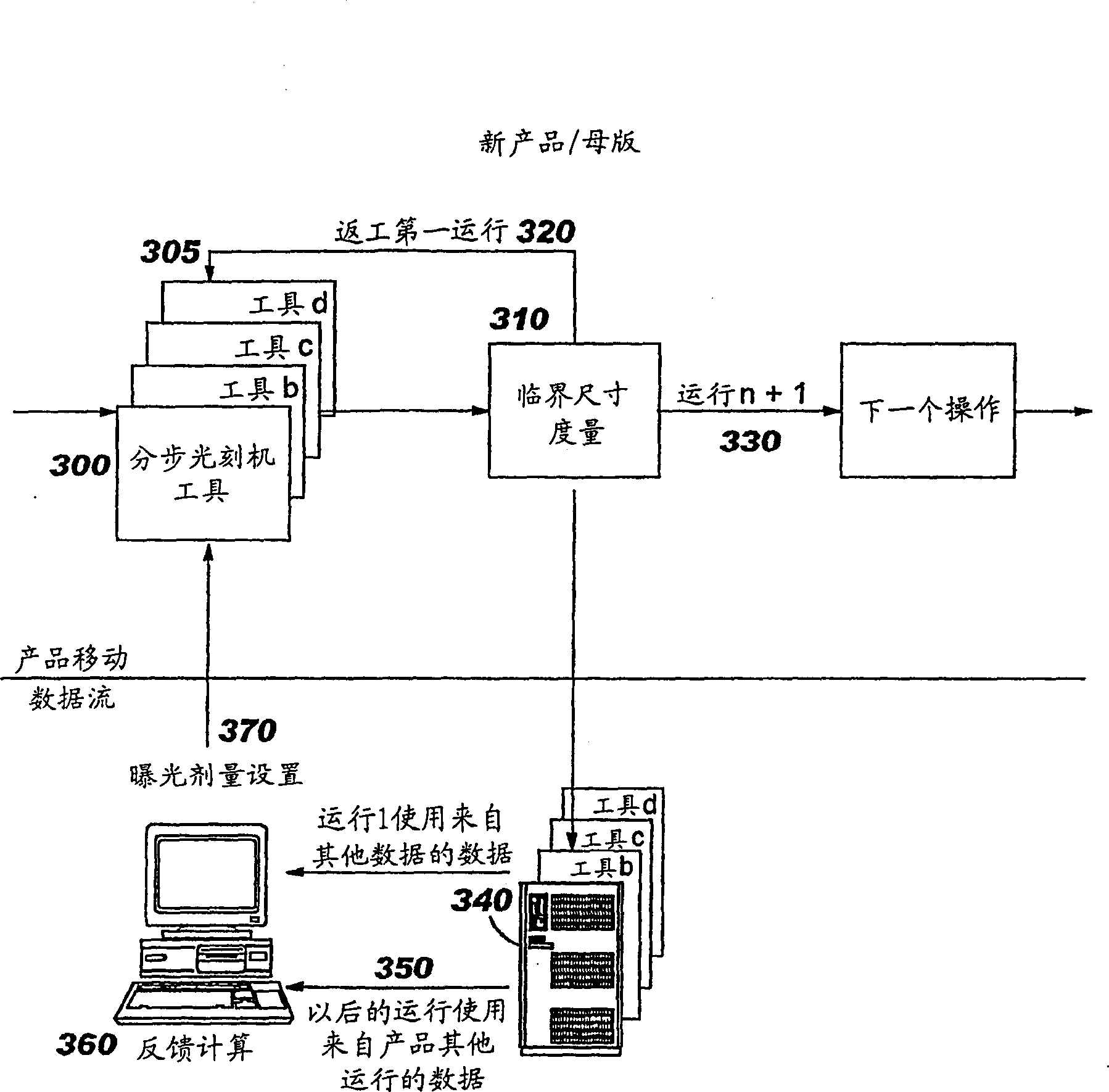
[0036] According to the present invention, it will be described as Figure 4 The system ( 490 ) shown in FIG. 2 , wherein the metrology data obtained in the critical dimension metrology step 420 is recorded as product history data 430 . This data is algorithmically mixed with master CD data 440 of similar masters (ie masters of the same technology and level) as part of a feedback calculation 450 to adjust exposure dose settings. The initial exposure dose calculated by the present invention does not require first-run rework for making production runs. Master dimension data, master factors, historical wafer exposure conditions, and historical wafer dimension data are stored in a database for each master. These data are used when a specific master is required for a given run.

[0037] It should be noted that the present invention can be used in lithographic techniques including proximity printing as well as projection printing. However, the present invention can be used with a...


PUM


Abstract

A method of implementing a new reticle for manufacturing semiconductors on a wafer which involves performing measurements on the reticle and assigning an initial exposure dose by using a predetermined algorithm. The exposure control system utilizes reticle CD data for automatically calculating reticle exposure offset values, i.e. reticle factors. A correlation of reticle size deviations to calculated reticle factors is used to derive a reticle factor for the new reticle. The derived reticle factor is then used to predict an initial exposure condition for the new reticle which is applied to the lithography tool for achieving a wafer design dimension.

Description

technical field [0001] The present invention relates generally to the field of lithography; more particularly, to a method of achieving wafer design dimensions through a process control system using simple control algorithms and feedback. This feedback uses mask design data, mask dimension data, and historical wafer pattern measurements to center the critical dimension (CD) to the wafer pattern design dimensions. The present invention provides a way to control the feature size, ie critical dimension of lines or spaces, by ensuring that each wafer is processed using the correct exposure conditions, using different master measurements. Background technique [0002] In the field of integrated circuits (ICs), photolithography is used to transfer patterns, or images, from masks containing circuit design information to thin films on the surface of a substrate, such as a silicon wafer. Pattern transfer is accomplished with the aid of photoresists such as UV-sensitive organic polym...

Claims


Application Information

Patent Timeline
Patent Type & Authority Patents(China)
IPC IPC(8): G03C5/00G06F19/00G21K5/00G06F17/50G01D18/00G03F7/20H01L21/027
CPCG03F7/70508G03F7/70558G03F7/70625
Inventor 杰迪·H·兰金克雷恩·E·施奈德约翰·S·史密斯安德鲁·J·沃茨
Owner GLOBALFOUNDRIES INC
Why Eureka
Try Eureka