A Method of Optical Proximity Correction for Mask

A technology of optical proximity correction and mask plate, which is applied in the direction of optics, photographic process of pattern surface, original for photomechanical processing, etc., can solve the problem of not getting accuracy, difficult to obtain target CD, and narrowing depth of field And other issues

Active Publication Date: 2016-07-06
SEMICON MFG INT (SHANGHAI) CORP
View PDF5 Cites 0 Cited by
  • Summary
  • Abstract
  • Description
  • Claims
  • Application Information

AI Technical Summary

Problems solved by technology

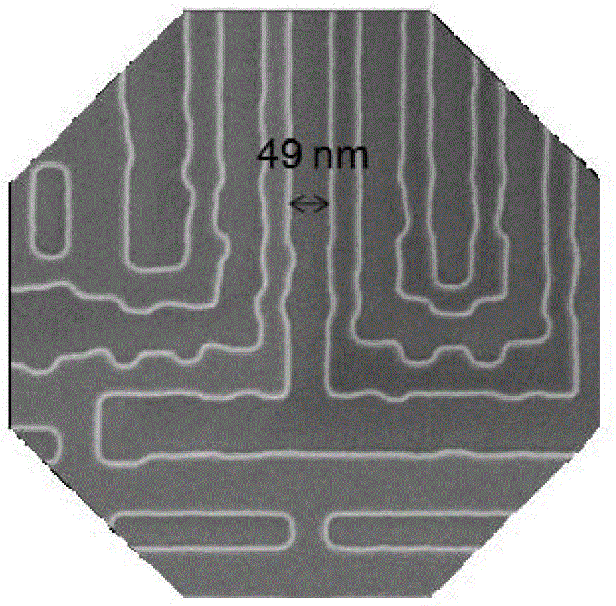
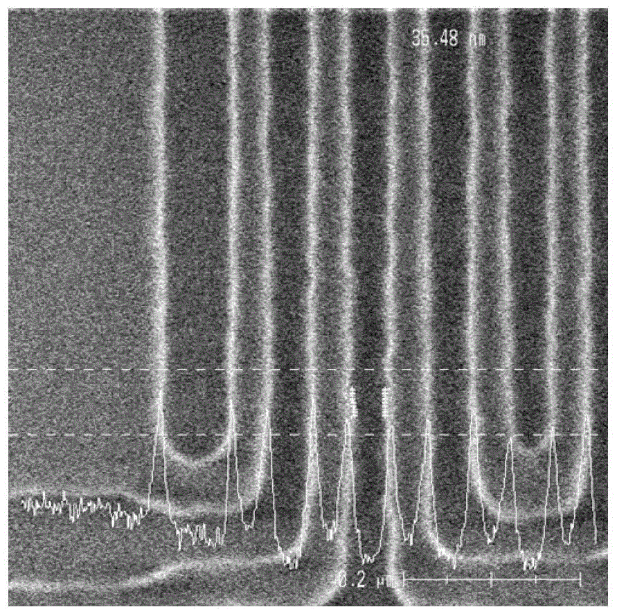
[0004] With the continuous shrinking of semiconductor integrated circuit CDs, the lithography resolution R must be increased to meet the requirements of the process. According to the formula of Rayleigh's law R=K1λ / NA and DOF=K2λ / (NA)2, where λ is the wavelength, K1 and K2 are constants, and NA is the numerical aperture of the imaging system. It can be seen that the way to improve the resolution is: reduce the wavelength and increase the NA, but this will cause the depth of field to shrink. With the decrease of K1, Mask error enhancement factor (maskrrorenhancedfactor, MEEF) increases, causing larger errors in lithography, more likely to cause distortion, and it is difficult to obtain a stable target CD, such as figure 1 and 2 as shown in figure 1 In the pattern whose target CD is 50nm, the CD obtained on the mask plate is 49nm, but the CD obtained on the wafer after photolithography through the mask plate is 35nm, while the desired CD on the wafer is 35nm. The CD to be obtained is 45nm, so there is a large error. The mask error enhancement (MEEF) factor is 10. When the MEEF is large, OPC will not get good accuracy in time. When the device When the size is further reduced, it is difficult to ensure the stability of the prepared device CD when the MEEF is large, thereby reducing the device preparation efficiency

Method used


Image

  • A Method of Optical Proximity Correction for Mask
  • A Method of Optical Proximity Correction for Mask
  • A Method of Optical Proximity Correction for Mask

Examples


Embodiment Construction

[0027] In the following description, numerous specific details are given in order to provide a more thorough understanding of the present invention. It will be apparent, however, to one skilled in the art that the present invention may be practiced without one or more of these details. In other examples, some technical features known in the art are not described in order to avoid confusion with the present invention.

[0028] It should be noted that the terms used herein are for the purpose of describing specific embodiments only, and are not intended to limit exemplary embodiments according to the present invention. As used herein, singular forms are intended to include plural forms unless the context clearly dictates otherwise. In addition, it should also be understood that when the terms "comprising" and / or "comprising" are used in this specification, it indicates the presence of the features, integers, steps, operations, elements and / or components, but does not exclude th...


PUM


Abstract

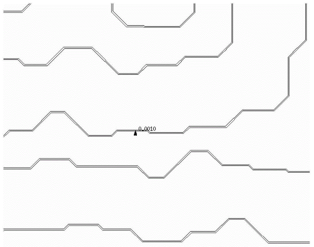
The invention relates to an optical proximity correction method for a mask, comprising: 1) preparing a mask pattern and performing optical proximity correction to obtain a corrected mask pattern; 2) enlarging the outline of the corrected mask pattern to obtain enlarging the mask pattern; 3) performing profile simulation on the enlarging mask pattern to obtain the enlarging mask graphic outline; 4) analyzing the CD of the enlarging mask enlarging outline to obtain the CD difference -ΔCD , the ΔCD is equal to the MEEF of the corrected mask pattern; 5) analyzing the MEEF, and marking the region with a large MEEF. In the present invention, the MEEF on the wafer is reduced by processing the area with larger MEEF when preparing the mask, and then the mask is exposed, so that the CD error is reduced, the target pattern is obtained, and at the same time, the Distortion of patterns and circuits.

Description

technical field [0001] The invention relates to the field of semiconductors, and in particular, the invention relates to an optical proximity correction method for a mask. Background technique [0002] Integrated circuit manufacturing technology is a complicated process, and the technology is updated very quickly. A key parameter that characterizes integrated circuit manufacturing technology is the minimum feature size, that is, critical dimension (CD). Smallness makes it possible to have millions of devices per chip. [0003] Photolithography is the driving force behind the development of integrated circuit manufacturing processes, and it is also one of the most complex technologies. Compared with other single manufacturing technologies, the improvement of lithography technology is of great significance to the development of integrated circuits. Before the lithography process starts, it is first necessary to copy the pattern on the mask plate through specific equipment, ...

Claims


Application Information

Patent Timeline
Patent Type & Authority Patents(China)
IPC IPC(8): G03F1/36
Inventor 王辉
Owner SEMICON MFG INT (SHANGHAI) CORP
Why Eureka
Try Eureka