

Liquid crystal display device
A liquid crystal display device, black display technology, applied in the directions of instruments, polarizing elements, optics, etc., can solve the problems of unconsidered and reduced light leakage, and achieve the effect of reducing color shift
Inactive Publication Date: 2008-06-25
FUJIFILM CORP
View PDF26 Cites 13 Cited by
- Summary
- Abstract
- Description
- Claims
- Application Information
AI Technical Summary
Problems solved by technology
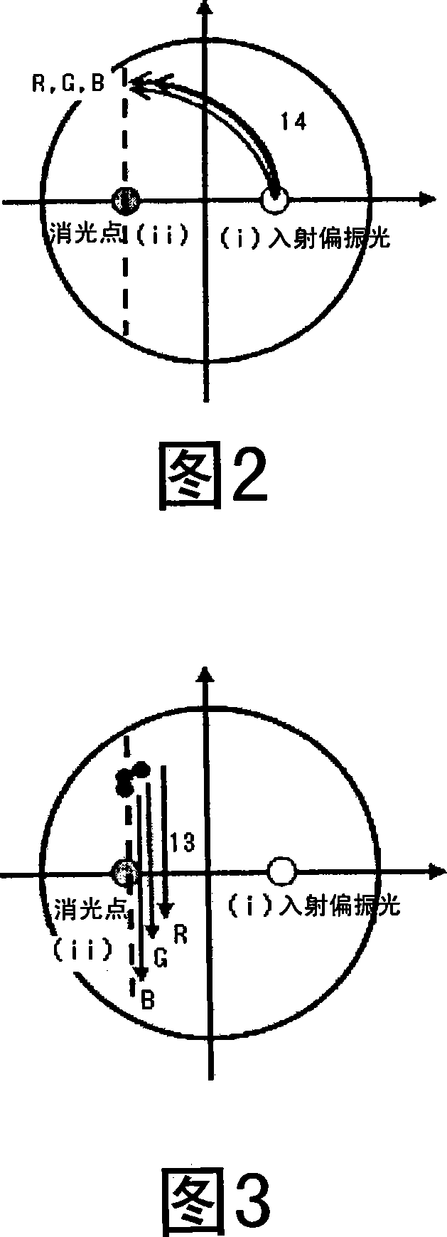
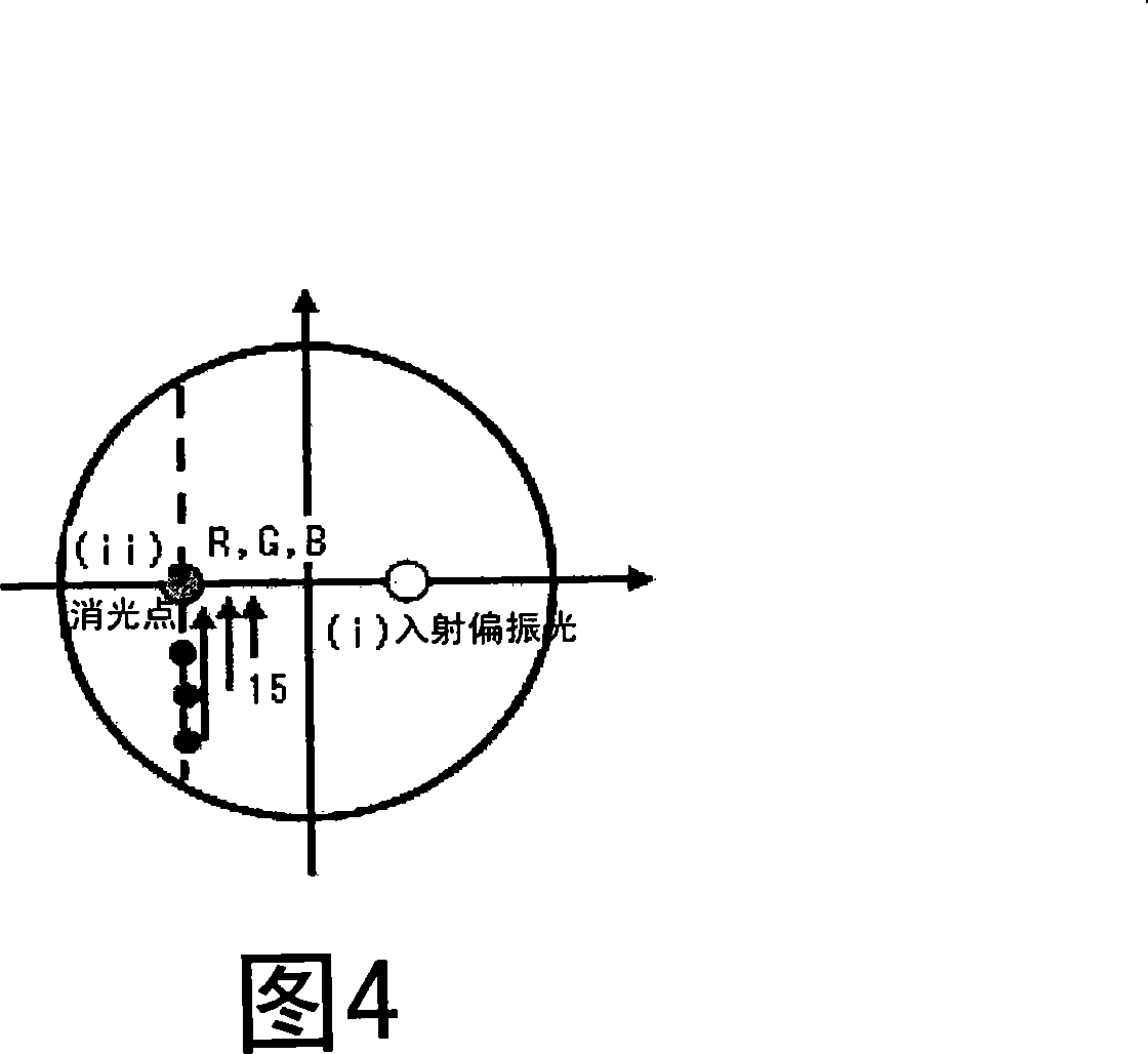
[0005] However, the above method only reduces light leakage for a certain wavelength range (for example, green light around 550nm), and does not consider light leakage for other wavelength ranges (for example, blue light around 450nm, red light around 650nm)
Method used
View moreImage
Smart ImageViewing Examples

Examples
specific example X-1
[0409]
specific example X-2
[0411]
specific example X-3
[0413]
Login to View More PUM
| Property | Measurement | Unit |
|---|---|---|
| thickness | aaaaa | aaaaa |
| elastic modulus | aaaaa | aaaaa |
| glass transition temperature | aaaaa | aaaaa |
Abstract
A liquid crystal display device comprising first and second polarizing elements of which transmission axes are perpendicular to each other, and, disposed between the polarizing elements, a liquid crystal layer vertically aligned in a black state, and first and second optically anisotropic layer is disclosed. In the liquid crystal display device, the first optically anisotropic layer is a biaxial optically anisotropic layer of which in-plane retardation (Re) and thickness-direction retardation (Rth) are larger at a longer wavelength range within a range of from 400 nm to 700 nm, and the second optically anisotropic layer satisfies Orim10 in which Re (550) is in-plane retardation (Re) at a wavelength of 550 nm and Rth (550) is thickness-direction retardation at the same wavelength.
Description
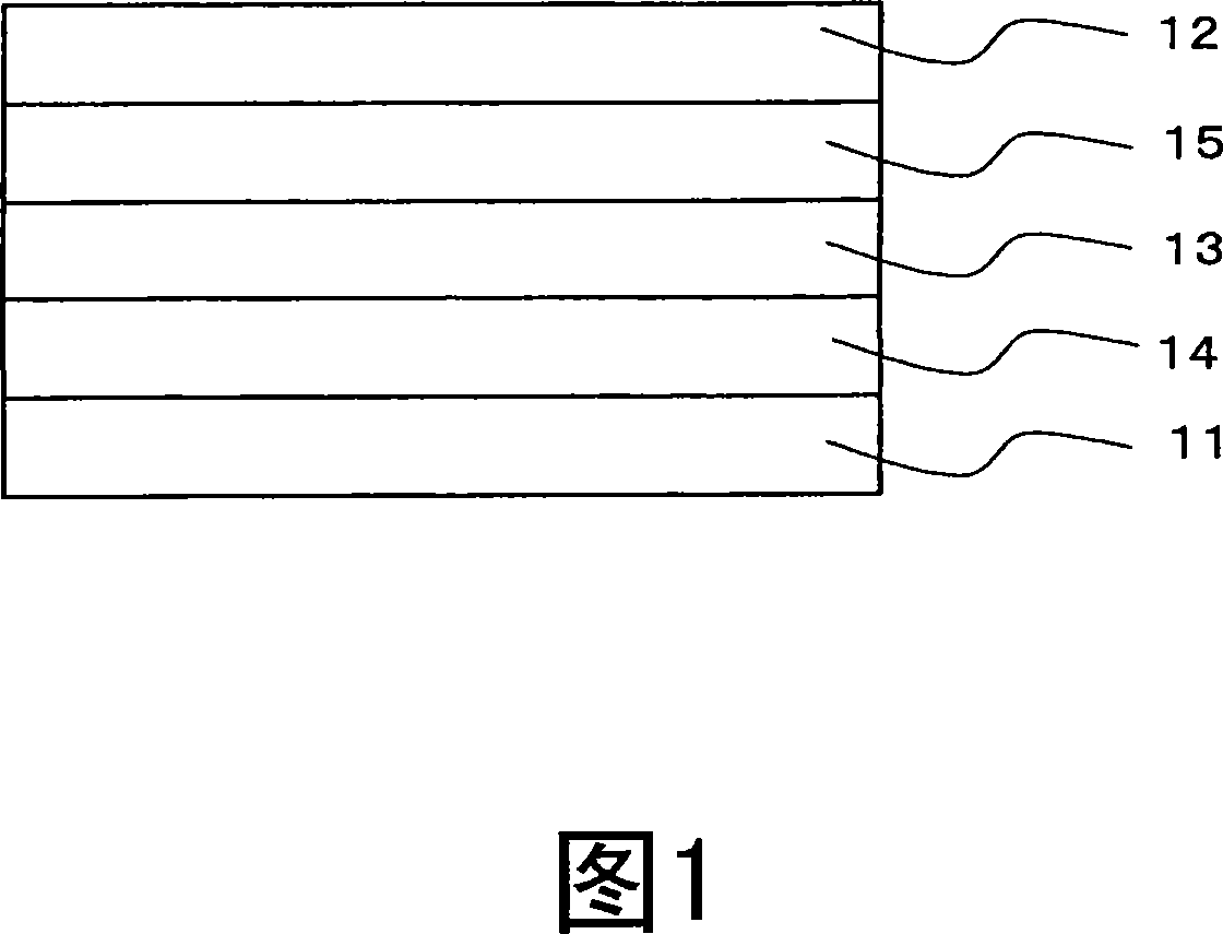
technical field [0001] The present invention relates to a liquid crystal display device with improved viewing angle characteristics. Background technique [0002] Liquid crystal display devices are widely used as monitors and televisions for personal computers and portable devices due to their various advantages such as low voltage, low power consumption, miniaturization, and thin film reduction. Various modes have been proposed for such liquid crystal display devices depending on the alignment state of liquid crystal molecules in the liquid crystal cell, but the TN mode, in which the alignment state is twisted approximately 90° from the lower substrate toward the upper substrate of the liquid crystal cell, has been the mainstream. [0003] Generally, a liquid crystal display device is composed of a liquid crystal cell, an optical compensation sheet, and a polarizer. Optical compensation sheets are used to eliminate coloring of images and to expand viewing angles, and films...
Claims
Login to View More Application Information
Patent Timeline
 Patent Type & AuthorityApplications(China)
IPC IPC(8): G02F1/13363G02F1/1335G02B1/04G02B1/10G02B5/30
CPCG02F1/133634G02B5/3083G02F2203/64G02F1/1335
Inventor远山浩史保田浩太郎中山元深川伸隆田口庆一
OwnerFUJIFILM CORP