Buffer circuit

A buffer and circuit technology, applied in the direction of logic circuits, logic circuits with logic functions, logic circuit connection/interface layout, etc., can solve the problems of lower system efficiency and poor noise tolerance of digital circuits, and achieve high operating frequency Wide, poor noise suppression tolerance, less clock pulse jitter effect

Inactive Publication Date: 2008-06-25
IND TECH RES INST
View PDF1 Cites 4 Cited by
  • Summary
  • Abstract
  • Description
  • Claims
  • Application Information

AI Technical Summary

Problems solved by technology

However, digital circuits can suffer from poor noise tolerance
Also, when digital circuits operate at high frequencies, the resulting switching noise can reduce system efficiency

Method used


Image

  • Buffer circuit
  • Buffer circuit
  • Buffer circuit

Examples


Embodiment Construction

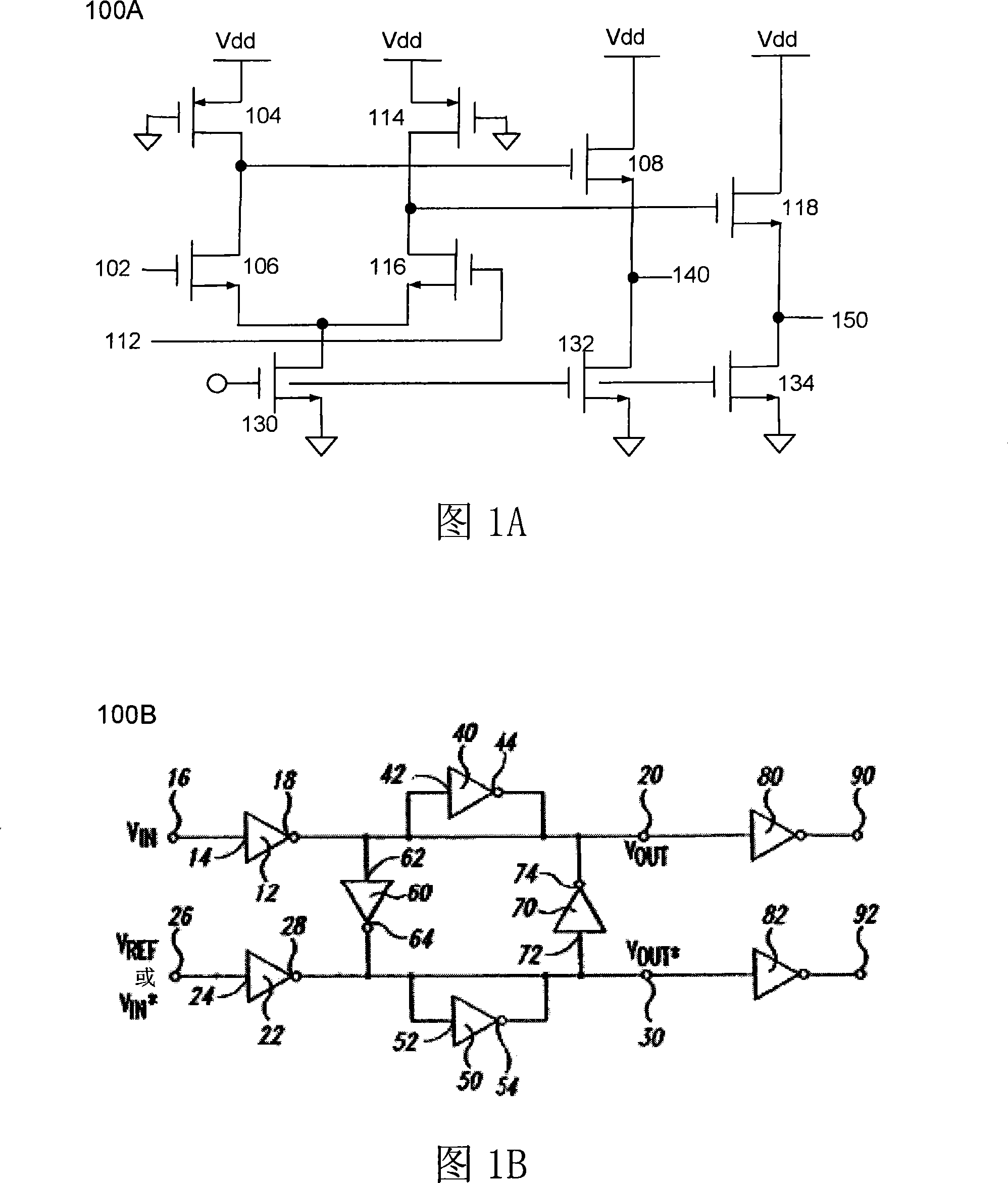
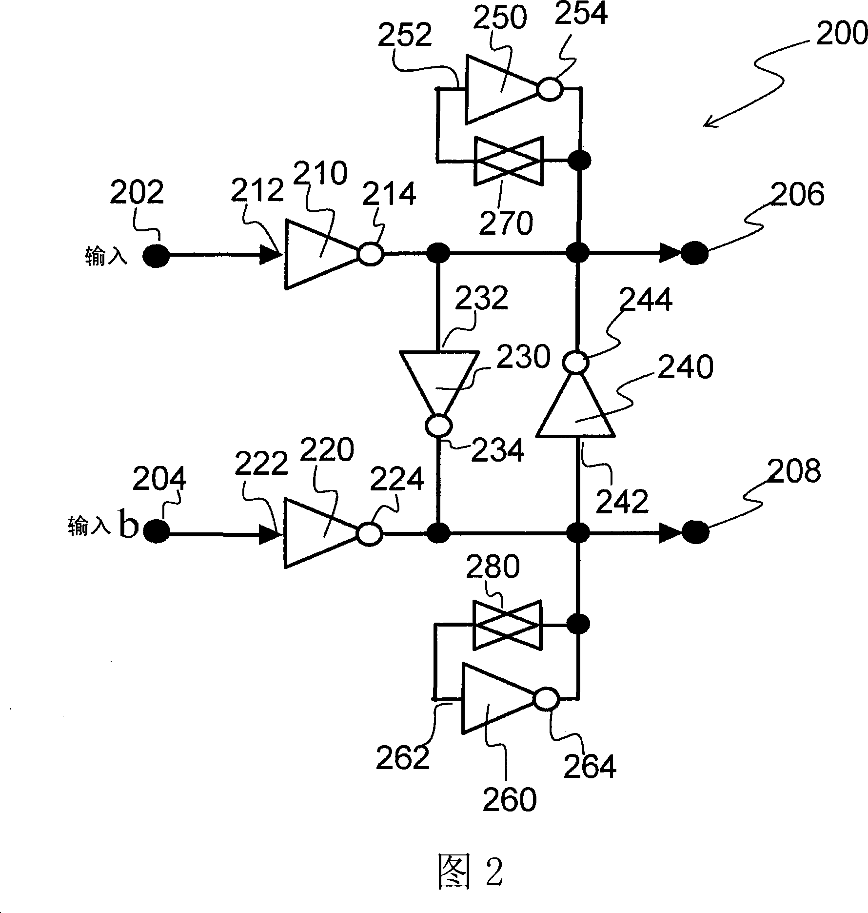
[0113] In order to have a further understanding of the purpose, structure, features, and functions of the present invention, it will be described in detail below with reference to the accompanying drawings and examples, but the following drawings and examples are only for auxiliary illustrations, and the present invention is not limited to the accompanying drawings and examples. FIG. 2 is an exemplary circuit diagram of a buffer circuit 200 in an example according to the present invention. The buffer circuit may have a first input terminal 202 , a second input terminal 204 , a first output terminal 206 and a second output terminal 208 . The first input terminal 202 can be coupled to the input signal V in . The first output terminal 206 can provide an output signal V out . The second input terminal 204 can be coupled to the complementary input signal V in * , in this case, terminal 208 acts as a complementary output terminal to provide a complementary output signal V out...


PUM


Abstract

A buffer circuit having an input terminal and an output terminal comprises a first inverter having an input node coupled to the input terminal and an output node coupled to the output terminal, a second inverter having an input node coupled to a reference voltage and an output node, a third inverter having an input node coupled to the output terminal and an output node coupled to the output node of the second inverter, a fourth inverter having an input node coupled to the output node of the second inverter and an output node coupled to the output terminal, a fifth inverter having an input node and an output node coupled to the output terminal, a sixth inverter having an input node and an output node coupled to the output node of the second inverter, a first resistive element is coupled between the output terminal and the input node of the fifth inverter, and a second resistive element is coupled between the output node of the second inverter and the input node of the sixth inverter.

Description

technical field [0001] The present invention relates to a buffer circuit, in particular to a buffer circuit that can be used in a digital device (Digital device) or a system. Background technique [0002] Buffers are commonly used in data transmission systems. For example, signal buffer circuits may be used at an input interface to receive or amplify signals, enhance signal drive performance, and / or reduce signal transition times. [0003] Snubber circuits are often designed using analog circuits. An example of an analog buffer circuit may include a differential pair with several passive devices, including inductors, capacitors, and resistors. FIG. 1A shows a forward emitter coupled logic (PECL) analog buffer circuit 100A. PECL buffer 100A of FIG. 1A has input terminals 102 and 112 that receive independent PECL signals that are complementary to each other. The input terminal 102 is connected to a gate (Gate) of an NMOS transistor 106 , and the NMOS transistor (NMOS trans...

Claims


Application Information

Patent Timeline
Patent Type & Authority Applications(China)
IPC IPC(8): H03K19/0175H03K19/0185H03K19/20
CPCH03K19/00323H03K19/018571H04L25/028H03K19/01707H04L25/0272
Inventor 吕鸿文苏朝琴
Owner IND TECH RES INST
Why Eureka
Try Eureka