LCD device array substrate, its mending method and LCD device

A technology for liquid crystal display devices and array substrates, applied in the directions of optics, instruments, electrical components, etc., can solve problems such as unfavorable effective utilization of liquid crystal display panels, and achieve the effect of reducing the area

Active Publication Date: 2008-07-09
KUSN INFOVISION OPTOELECTRONICS
View PDF1 Cites 38 Cited by
  • Summary
  • Abstract
  • Description
  • Claims
  • Application Information

AI Technical Summary

Problems solved by technology

[0008] However, in the prior art shown in FIG. 2 and FIG. 3, the repair circuit 223 and the detection circuit 15 are independently arranged on the periphery of the display area 112, so a larger area is required in the liquid crystal display panel for this purpose. Such wiring cannot be used for display, which is not conducive to the effective use of liquid crystal display panels

Method used


Image

  • LCD device array substrate, its mending method and LCD device
  • LCD device array substrate, its mending method and LCD device
  • LCD device array substrate, its mending method and LCD device

Examples


Embodiment Construction

[0024] Exemplary embodiments of the present invention will be described in detail below with reference to the accompanying drawings.

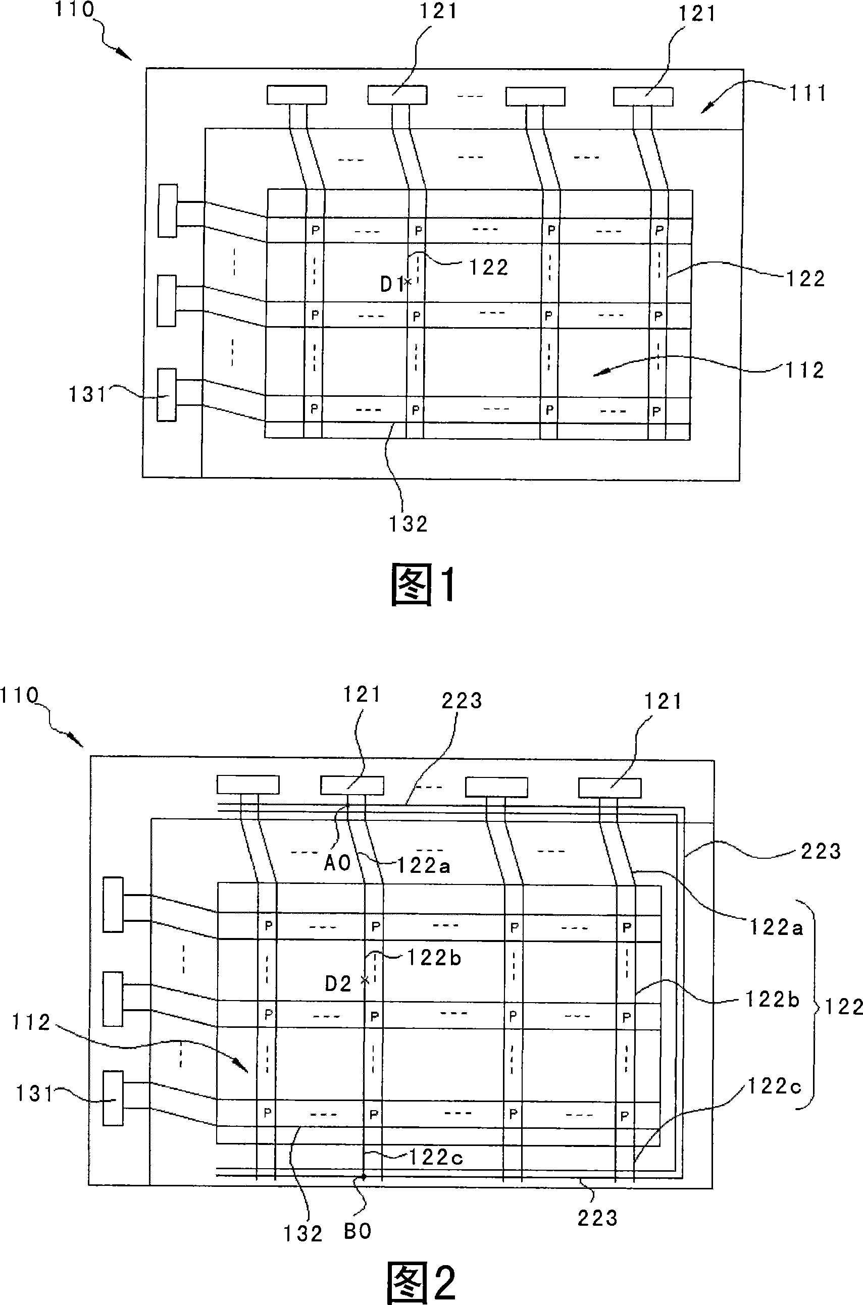
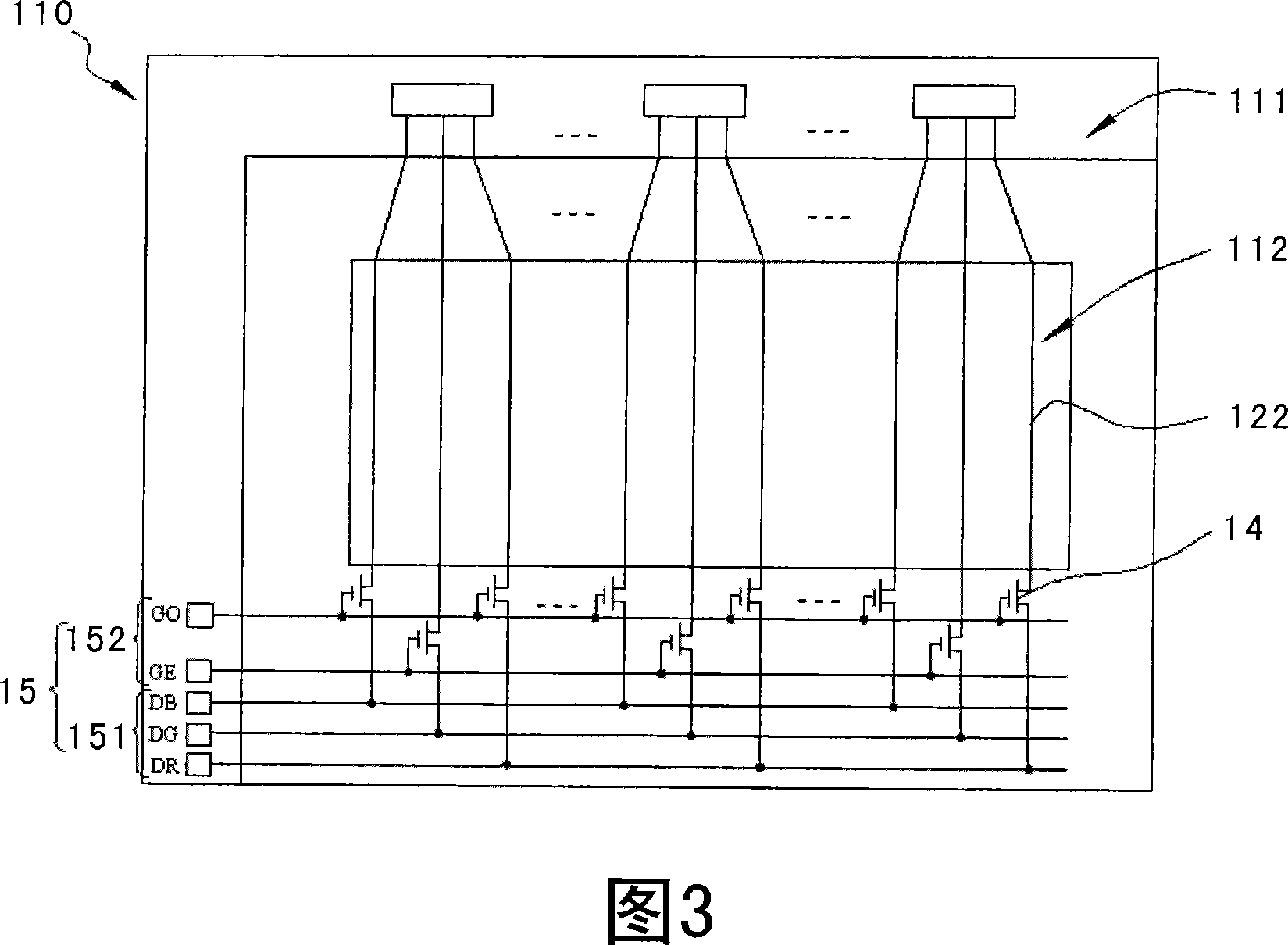
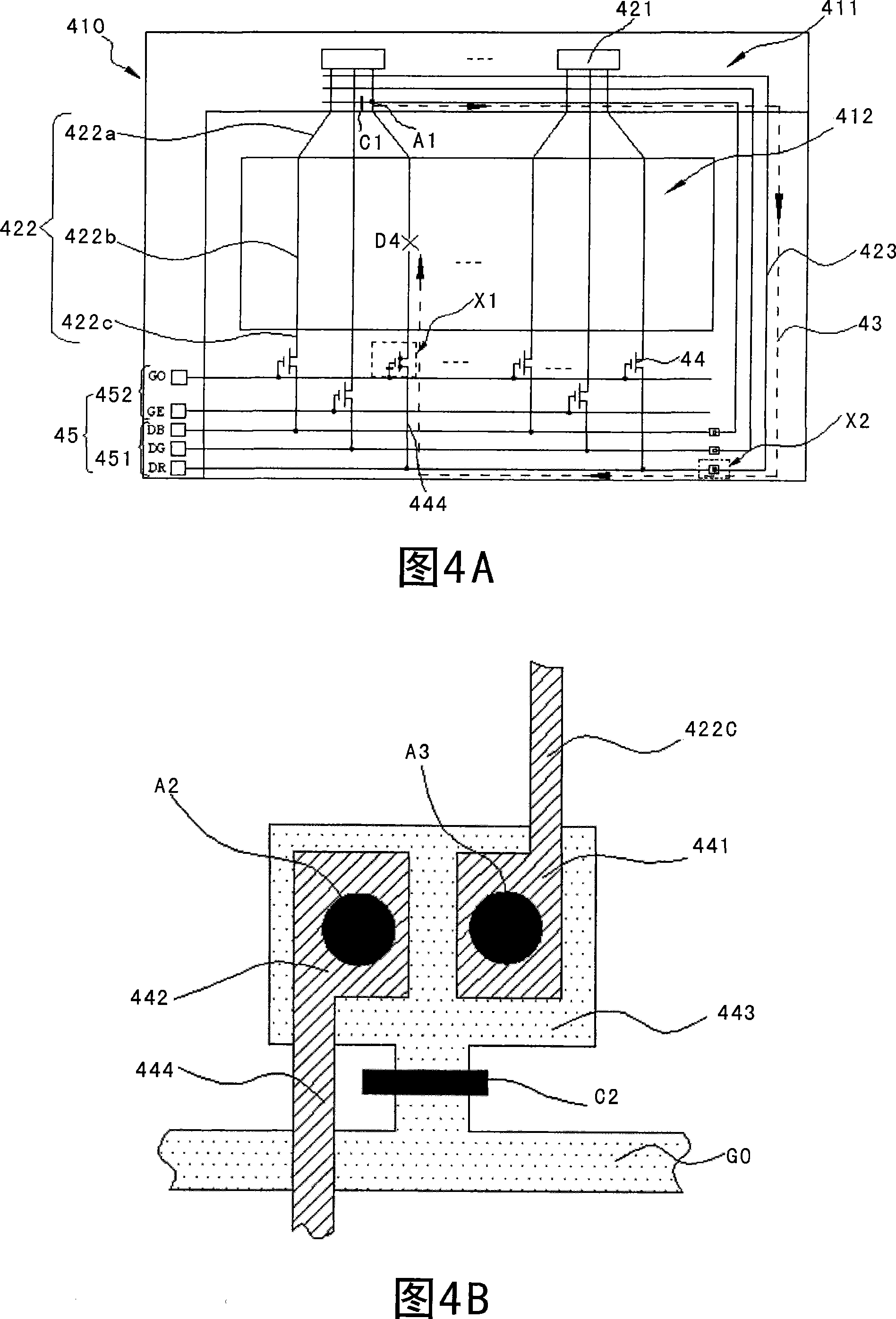
[0025] FIG. 4A is a schematic top view of a repair circuit structure of an array substrate of a liquid crystal display device according to a first embodiment of the present invention. The array substrate 410 of the liquid crystal display device includes a display area 412 and a signal introduction area 411 located on the periphery of the display area 412 , a plurality of data line pads 421 are formed in the signal introduction area 411 and electrically connected to each data line 422 respectively. Each data line 422 includes three parts, that is, the front data line part 422a located outside the display area 412 and electrically connected to the corresponding data line pad 421, the display area data line part 422b located in the display area 412, and the display area data line part 422b located in the display area. The end data line portion 422...


PUM


Abstract

The invention discloses an LCD device array substrate, which comprises a data line; a scan line arranged to intersect the data line; a detection line assembly arranged at the periphery of a display region in the array substrate, at least a portion of the detection line assembly being used for detecting the array substrate; and a repair line assembly arranged at the periphery of the display region for repairing defects of defective data line of the data lines, wherein the detection line assembly is so arranged that the detection line assembly is electrically isolated from the repair line assembly when not carrying out repair operation and that the detection line assembly is electrically connected with the repair line assembly and the defective data line during repairing. The invention also discloses the repair method of the LCD device array substrate and an LCD device using the array substrate. According to the invention, the detection line assembly can be used as a portion of the repair circuit to repair the data line, thus significantly reducing the area of the non-display region.

Description

technical field [0001] The invention relates to an array substrate of a liquid crystal display device and a repairing method thereof, in particular to an array substrate of a liquid crystal display device with a repaired circuit structure and a repairing method thereof, and also relates to a liquid crystal display device having the array substrate. Background technique [0002] Liquid crystal display devices have the advantages of lightness, thinness, and low power consumption, so they are widely used in modern information equipment such as notebook computers, mobile phones, and personal digital assistants. [0003] FIG. 1 is a schematic diagram of an array substrate in a conventional liquid crystal display device. The array substrate 110 of the liquid crystal display device includes a signal introduction area 111 and a display area 112 . Data line pads 121 and scan line pads 131 are formed in the signal lead-in area 111, a plurality of data lines 122 and scan lines 132 are ...

Claims


Application Information

Patent Timeline
Patent Type & Authority Applications(China)
IPC IPC(8): G02F1/1362G02F1/13H01L27/12
CPCG02F1/136259G02F2001/136263G02F1/136263
Inventor 钟德镇简廷宪廖家德
Owner KUSN INFOVISION OPTOELECTRONICS
Why Eureka
Try Eureka