Image element structure and LCD with the same
A technology of liquid crystal display and pixel structure, applied in instruments, nonlinear optics, optics, etc., can solve the problem of uneven brightness of liquid crystal display
- Summary
- Abstract
- Description
- Claims
- Application Information
AI Technical Summary
Problems solved by technology
Method used
Image
Examples
Embodiment Construction
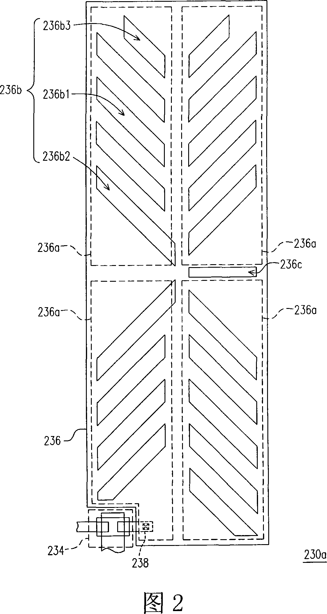
[0062] FIG. 2 is a schematic top view of a pixel structure of the present invention. Please refer to FIG. 2 , in this embodiment, each pixel structure 230 a includes an active device 234 and a pixel electrode 236 . The pixel electrode 236 is electrically connected to the active device 234 . In this embodiment, the pixel electrode 236 is electrically connected to the active device 234 through the contact window 238 , for example. The pixel electrode 236 is divided into a plurality of alignment regions 236a, and each alignment region 236a has a group of alignment slits 236b with the same alignment direction, and the alignment slits 236b adjacent to the alignment regions 236a have a symmetrical alignment direction, wherein Each group of alignment slits 236b includes a first alignment slit 236b1 and a second alignment slit 236b2, wherein the number of the first alignment slit 236b1 is the largest and the length is the same, and the alignment slit 236b of at least one of the align...
PUM
 Abstract
Description
Claims
Application Information


