Wafer adsorption mechanism

A technology of adsorption mechanism and wafer, applied in electrical components, semiconductor/solid-state device manufacturing, circuits, etc., can solve the problems of loss of detection accuracy and easy deformation of the substrate, saving manpower, reducing requirements, and reasonable and reliable structural design. Effect

Inactive Publication Date: 2008-07-16
THE 45TH RES INST OF CETC
View PDF0 Cites 14 Cited by
  • Summary
  • Abstract
  • Description
  • Claims
  • Application Information

AI Technical Summary

Problems solved by technology

[0009] The purpose of the present invention is to provide a wafer adsorption mechanism, to solve the technical problem of making a working surface adaptable to wafers of various specifications; and to solve the technical problems of traditional substrate detection accuracy loss, easy deformation, etc.

Method used


Image

  • Wafer adsorption mechanism
  • Wafer adsorption mechanism
  • Wafer adsorption mechanism

Examples


Embodiment Construction

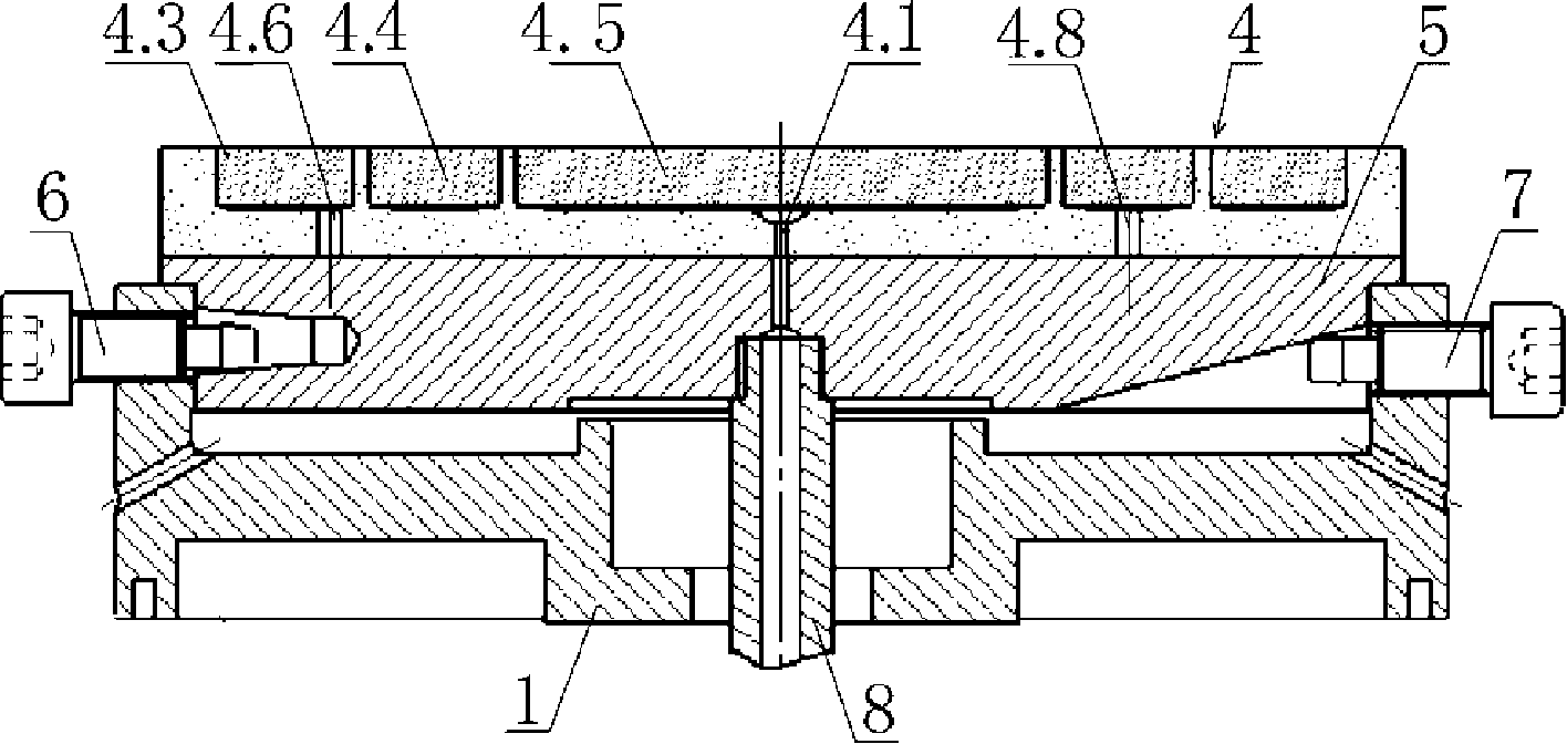
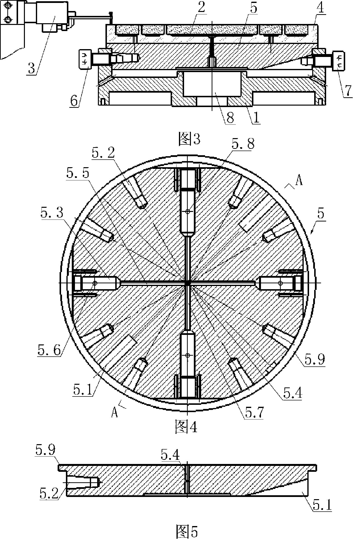
[0041] Examples see figure 1 As shown in -3, this wafer adsorption mechanism includes a mounting plate 1, a base plate 4 on the mounting plate and a vacuum system, and the online detector 3 is generally located at the edge of the base plate 4. An air duct 8 is connected from the mounting plate to the base plate 4 .

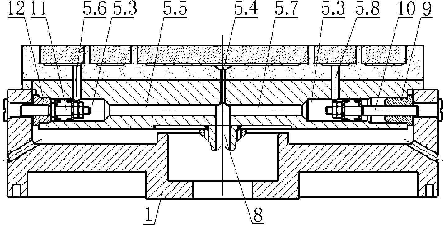
[0042] Referring to Fig. 4-5, there is an adjustment bottom plate 5 between the installation plate 1 and the base plate 4. The adjustment bottom plate 5 requires high machining accuracy, and the material is 3Cr13. The adjustment bottom plate 5 is supported on the bottom of the base plate 4, wedge-shaped lifting grooves 5.1 are symmetrically distributed on the edge of the bottom surface of the adjustment bottom plate 5, fastening screw holes 5.2 are evenly opened on the sides of the adjustment bottom plate 5, and the center of the adjustment bottom plate 5 is opened with The central hole 4.1 of the base plate corresponds to the central hole 5.4 of the adjustment b...


PUM


Abstract

The invention provides a wafer adsorption mechanism, wherein an adjusting bottom board is arranged between a mounting disk and a basal disc, wherein, edges of the bottom of the adjusting bottom board are symmetrically distributed with raised grooves, side edges of the adjusting bottom board are evenly provided with fastening screws, the center of the adjusting bottom is provided with a centre bore of the adjusting bottom board, a long air duct and a short air duct which are crossed at the centre bore of the adjusting bottom board, wherein, the upper wall of a screw hole of the long air duct is provided with a larger annular adjusting hole, the upper wall of a screw hole of the short air duct is provided with a middle annular adjusting hole; the large annular adjusting hole fitly connected with a short adjusting screw nut and a short adjusting component, the middle annular adjusting hole is fitly connected with a long adjusting screw nut and a long adjusting component, screw outer rings of the long adjusting component and the short adjusting component are provided with pistons and seal rings. The basal disc is made of porous ceramic materials, wherein, the internal bottom surface of the basal disc is provided with a centre hole of the basal disc, a concentric ring air duct groove, a large ring compress hole, an inter-ring air duct and a middle ring compress hole, the outer ring of the internal bottom surface of the basal disc is pasted with a large vacuum ring, and the middle ring of the internal bottom surface of the basal disc is pasted with a middle vacuum ring, and the center of the internal bottom surface of the basal disc is pasted with a small vacuum disk, and the install disk and the adjusting bottom board are tightly connected. The mechanism can adsorb 3 to 8 wafers only through simple adjustment.

Description

(1) Technical field [0001] The invention relates to a disk adsorption workbench, in particular to a wafer adsorption mechanism used in the semiconductor equipment manufacturing industry. (2) Background technology [0002] In the semiconductor equipment manufacturing industry, there are multiple technological processes for wafer processing. In these technological processes, a working surface for absorbing wafers is required. Many semiconductor equipment manufacturers use one specification of wafers to match one kind of work for the important mechanism of wafer adsorption. Table, when processing wafers with different specifications, there is a complicated process of replacing the work table. In the process of replacing the work table, there are the following problems: [0003] 1. The positioning accuracy of the workbench is lost. [0004] 2. Uncertain factors such as duplication of structure and storage cause excessive price and waste. [0005] 3. High-level skilled personne...

Claims


Application Information

Patent Timeline
Patent Type & Authority Applications(China)
IPC IPC(8): H01L21/683
Inventor 王广峰王仲康柳滨
Owner THE 45TH RES INST OF CETC
Why Eureka
Try Eureka